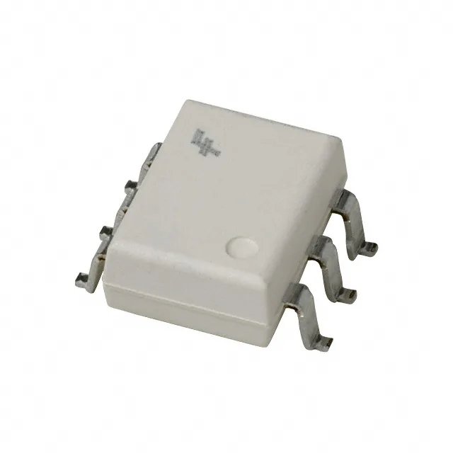
What the MOSFET output buys you in isolation design
The H11F1SM is a single-channel optoisolator with a MOSFET output stage, not a phototransistor. That means the output behaves as a voltage-controlled resistor — no offset voltage, no saturation voltage — so it can pass analog signals from DC up to a few kilohertz without the Vce(sat) error a transistor output would introduce. The 4170 Vrms isolation rating is the galvanic barrier between the input LED and the output FET, tested per the 6-SMD Gull Wing package's creepage distance.
Switching speed and drive current budget
Turn-on and turn-off times are both 45 µs max — symmetrical, which simplifies timing in low-frequency multiplexed or sample-hold circuits. The forward voltage is 1.3 V typ, and the LED can be driven up to 60 mA continuous. At 10 mA forward current the switching times stay near the typical value; pushing to 60 mA reduces turn-on slightly but increases LED stress. The 30 V max output voltage limits the FET drain-to-source swing — fine for 5 V or 12 V logic-level loads, but not for 24 V industrial rails.
Temperature grade and board environment
The DC input type means the LED is polarity-sensitive; reverse voltage protection on the input side is the designer's responsibility.