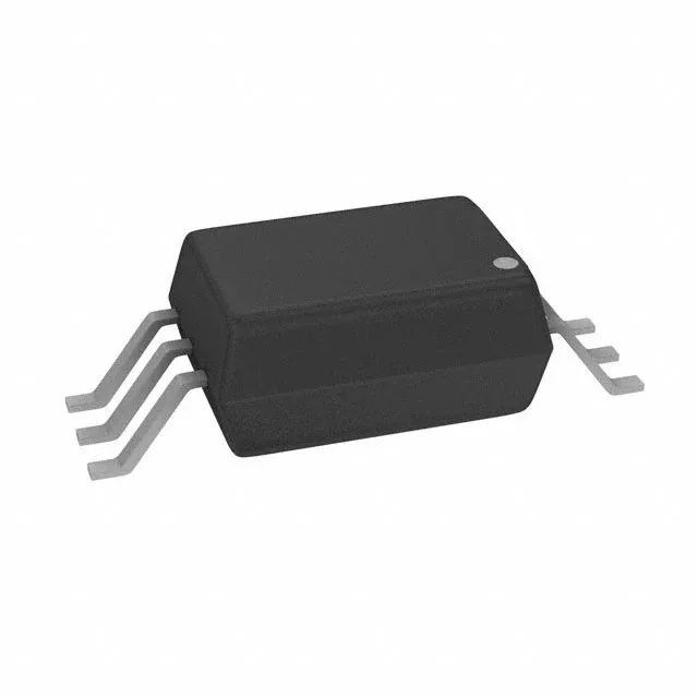
What the 5000Vrms and 4A peak ratings mean for your gate-drive design
The FOD8343TR2 is a single-channel optocoupled gate driver from onsemi that delivers 4A peak output current across a 5000Vrms reinforced isolation barrier. That isolation rating is the safety envelope for motor-drive, inverter, and industrial power-supply applications where the primary and secondary sides must stay galvanically separated. The 4A peak output is enough to drive medium-power IGBTs and MOSFETs directly — think 600V/20A class switches — without an external buffer stage.
Parametric deep-dive: propagation delay, CMTI, and pulse-width distortion
Propagation delay is 210ns max for both tpLH and tpHL, with pulse-width distortion held to 65ns max. That symmetry matters when the downstream gate needs a clean on/off transition — asymmetric delay shifts the duty cycle and can saturate the transformer core in a half-bridge topology. A driver with low CMTI can latch the output high or low, causing shoot-through. At 50kV/µs, the FOD8343TR2 stays quiet through that transient.
Supply voltage and output drive capability
The output side operates from 10V to 30V, which covers the standard gate-drive rails for IGBTs (typically 15V) and MOSFETs (10V to 15V). The high/low output current is rated 3A source and 3A sink, so the part can charge and discharge the gate capacitance at roughly equal rates. Rise and fall times are 38ns and 24ns typical — the faster fall time helps turn off the power switch cleanly, reducing the tail-current loss in IGBTs.