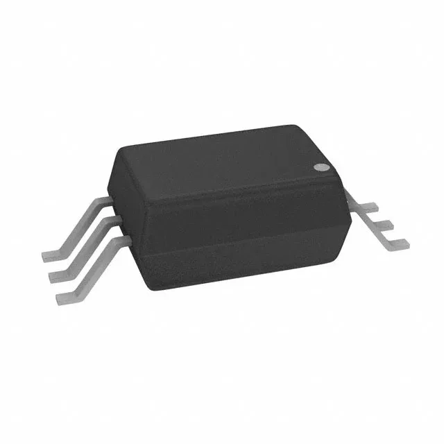
onsemi FOD8342R2 — Optoisolators

FOD8342R2 onsemi Optocoupler Gate Driver 5000Vrms 3A 6SOP

MPNFOD8342R2
End of Life

onsemi FOD8342R2, single-channel optical coupling gate driver, 5000Vrms isolation, 3A peak output, 2.5A sink/source, 20kV/µs CMTI, 6-SOP package, -40°C to 100°C operating range.

$2.74Ref. price · indicative, final on quote
Packaging6-SOIC (0.268", 6.80mm Width)
StockContact for availability
MOQ1 pcs
  • 100% new & originalTraceable channels only — no refurbs, no pulls, no remarked parts.
  • Date & lot codes on quoteStated per line before you commit; label photos on request.
  • MSL-compliant ESD packingMoisture-sealed bags with indicator cards; reels photo-verified.
  • PayPal buyer protectionPay by T/T, PayPal or Payoneer — card payments covered end to end.

Specifications

FOD8342R2 Technical Specifications
ParameterValue
Mounting typeSurface Mount
Voltage - isolation5000Vrms
Voltage - output supply10V ~ 30V
Voltage - forward (Vf)1.5V
Current - peak output3A
Current - output high, low2.5A, 2.5A
Current - DC forward (If)25 mA
Operating temperature-40°C ~ 100°C
Pulse width distortion65ns
Approval agencyUR
PackageTape & Reel (TR); Cut Tape (CT)
TechnologyOptical Coupling
Case6-SOIC (0.268\", 6.80mm Width)
Number of channels1
Rise (Fall time)38ns, 24ns
Propagation delay tpLH (tpHL)210ns, 210ns
Common mode transient immunity20kV/µs

Product details

Gate driver optocoupler with 5000Vrms isolation and 3A peak drive

The FOD8342R2 is a single-channel optocoupler gate driver from onsemi, designed to drive IGBTs and power MOSFETs in motor drives, inverters, and industrial power supplies. The 5000Vrms isolation rating provides reinforced insulation for safety-critical designs, while the 3A peak output and 2.5A symmetrical sink/source capability handle the gate charge of medium-power switches without an external booster stage.

Parametric deep-dive: timing, drive strength, and transient immunity

Propagation delay is 210ns max for both tpLH and tpHL, with pulse width distortion held to 65ns max — this keeps switching dead-time predictable and minimises asymmetry in half-bridge topologies. Rise and fall times are 38ns and 24ns typical, fast enough for switching frequencies up to several hundred kHz, though the actual frequency ceiling depends on total gate charge and supply voltage. Common mode transient immunity is rated at 20kV/µs minimum, which prevents false turn-on when high dv/dt transients couple across the isolation barrier in inverter legs. The output supply range is 10V to 30V, covering standard gate drive voltages for IGBTs (15V) and MOSFETs (12V-18V). Forward voltage is 1.5V typical with a 25mA maximum forward current, compatible with 3.3V and 5V logic interfaces through a series resistor.

Lifecycle, compliance, and sourcing

The part is ROHS3 compliant and carries UR agency approval.

Package and mounting

Housed in a 6-SOIC package with 0.268-inch body width (6.80mm), designated as 6-SOP by onsemi. Surface-mount assembly on standard SOIC-6 footprint. Supplied in Tape & Reel or Cut Tape for both prototyping and production reels.

Frequently asked questions

What is the maximum Vcc for FOD8342R2?

The output supply range is 10V to 30V. For 15V IGBT gate drive or 12V MOSFET drive, the part operates comfortably within this range.

Can FOD8342R2 drive a 1200V IGBT directly?

Yes, the 5000Vrms isolation provides the reinforced insulation needed for the high-side gate drive in a 1200V bus system. The 3A peak output and 2.5A sink/source are sufficient for medium-current IGBT modules; larger modules may require an external gate booster.