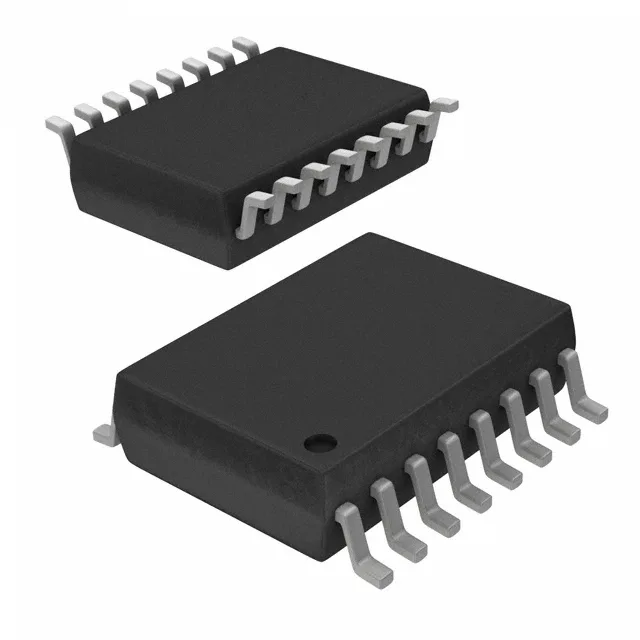
3 A gate driver with 4243 Vrms isolation for IGBT/MOSFET stages
The FOD8333R2 is a single-channel optocoupler gate driver from onsemi, rated for 3 A peak output current with 4243 Vrms isolation. That peak current is enough to drive medium-power IGBTs and MOSFETs directly — no external booster buffer needed for modules up to about 50 A rating at moderate switching frequencies. The 35 kV/µs minimum common-mode transient immunity keeps the output from false-triggering when the power-stage drain/collector voltage slews through the isolation barrier capacitance, a real concern in half-bridge inverter legs.
Switching speed and dead-time margin
For a 20 kHz switching inverter, the 250 ns propagation delay eats about 0.5% of the switching period — negligible for dead-time budgeting. The 2.5 A source/sink capability means the gate charge is delivered symmetrically, so turn-on and turn-off delays stay matched.
Supply range and forward LED drive
Output-side supply range is 3 V to 15 V, covering standard gate-drive voltages for both logic-level MOSFETs (5 V) and IGBTs (12–15 V). The input LED forward voltage is 1.45 V typical, with a maximum DC forward current of 25 mA — a 330 Ω series resistor from a 3.3 V or 5 V logic rail lands the LED current near 10–15 mA, well within the limit.
Package, MSL, and reflow considerations
Housed in a 16-SOIC wide-body package (0.295-inch body width, 7.50 mm), the FOD8333R2 uses a standard SOIC-16 footprint — no exotic pad geometry. ROHS3 compliant. For volume pricing and lead time, request a quote against your BOM quantity; we source per RFQ and confirm availability at quote time.