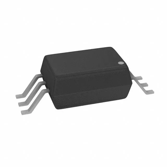
onsemi FOD8314R2 — Optoisolators

FOD8314R2 onsemi Optoisolator Gate Driver – 5000Vrms

MPNFOD8314R2
End of Life

onsemi FOD8314R2, single-channel optical coupling gate driver, 5000Vrms isolation, 1.5A peak output, 6-SOP surface-mount package, -40°C to 100°C.

$1.64Ref. price · indicative, final on quote
Packaging6-SOIC (0.268", 6.80mm Width)
StockContact for availability
MOQ1 pcs
  • 100% new & originalTraceable channels only — no refurbs, no pulls, no remarked parts.
  • Date & lot codes on quoteStated per line before you commit; label photos on request.
  • MSL-compliant ESD packingMoisture-sealed bags with indicator cards; reels photo-verified.
  • PayPal buyer protectionPay by T/T, PayPal or Payoneer — card payments covered end to end.

Specifications

FOD8314R2 Technical Specifications
ParameterValue
Mounting typeSurface Mount
Voltage - isolation5000Vrms
Voltage - output supply16V ~ 30V
Voltage - forward (Vf)1.5V
Current - peak output1.5A
Current - output high, low1A, 1A
Current - DC forward (If)25 mA
Operating temperature-40°C ~ 100°C
Pulse width distortion300ns
Approval agencyUL
PackageTape & Reel (TR); Cut Tape (CT)
TechnologyOptical Coupling
Case6-SOIC (0.268\", 6.80mm Width)
Number of channels1
Rise (Fall time)60ns, 40ns
Propagation delay tpLH (tpHL)500ns, 500ns
Common mode transient immunity20kV/µs

Product details

Active production — no LTB watch needed

onsemi lists the FOD8314R2 as Active. ROHS3 compliant — no exemption expiry to track.

5000Vrms isolation and 1.5A peak output

Rated for 5000Vrms isolation — sufficient for reinforced insulation in motor-drive and inverter applications where the gate-drive supply must float above the DC bus. The 1.5A peak output drives the gate charge of medium-power IGBTs and MOSFETs; the 1A source/sink capability handles the Miller plateau without excessive switching loss. Propagation delay is 500ns max with 300ns max pulse-width distortion — the timing skew is tight enough for dead-time management in half-bridge topologies.

20kV/µs CMTI for noisy switching environments

Common-mode transient immunity is 20kV/µs minimum. In a 600V inverter with 100ns voltage edges, the dV/dt at the isolation barrier exceeds 6kV/µs — the FOD8314R2's margin keeps the output from false-triggering. The 60ns rise / 40ns fall times match the gate-drive bandwidth for switching frequencies up to ~100 kHz.

6-SOP surface-mount package and supply range

Housed in a 6-SOIC (0.268", 6.80mm width) package, supplier device package 6-SOP. The 16V to 30V output supply range covers standard gate-drive rails for IGBTs (typically +15V turn-on, -5V to -10V turn-off via a bipolar supply). Operating temperature -40°C to 100°C suits industrial enclosures and outdoor cabinet environments.

Frequently asked questions

What is the closest functional second-source — FOD8332R2?

The FOD8332R2 (peer) is a higher-current variant: 2.5A peak output vs 1.5A, with 35kV/µs CMTI vs 20kV/µs, and 250ns propagation delay vs 500ns. Both are single-channel, surface-mount, UL-approved. The FOD8314R2 is the lower-cost option for designs that do not need the extra headroom.