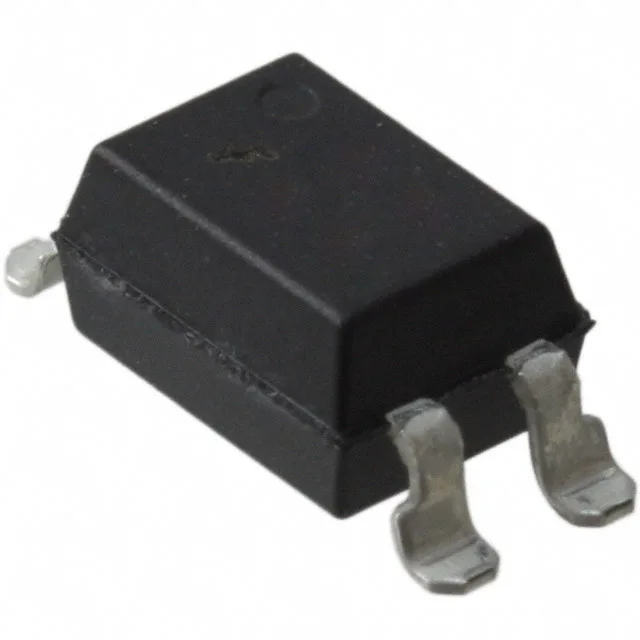
5000Vrms isolation defines the galvanic barrier
The FOD817BSD from onsemi provides 5000Vrms of input-to-output isolation, which is the primary design parameter for this part — it determines the working voltage and creepage distance on the PCB. In a motor-drive or PLC digital-input module, that 5 kV rating gives enough margin to separate the 24 V field side from the 3.3 V or 5 V logic side without arcing across the isolation barrier.
CTR range 130%–260% @5mA sets the logic interface margin
Current transfer ratio is specified at 5 mA forward current: minimum 130%, maximum 260%. That spread means at 5 mA in, the output transistor can sink between 6.5 mA and 13 mA into the load. For a typical 5 V logic input with a 10 kΩ pull-up, the required sink current is only 0.5 mA — so even the minimum CTR at cold temperature and worst-case LED degradation leaves substantial margin. The 200 mV maximum Vce(sat) keeps the output voltage low enough to be recognised as a solid logic low by any standard CMOS or TTL input. Rise and fall times are 4 µs and 3 µs typical, respectively. That limits the useful switching frequency to roughly 50–100 kHz for clean pulse transmission — fine for 50/60 Hz AC zero-cross detection, relay drive, or PLC input sampling, but too slow for high-speed data or PWM above a few hundred kHz.
The base product number FOD817 is a long-running onsemi series with multiple CTR and package variants, which means replacement within the family is straightforward if a different CTR bin is needed. Tape-and-reel and cut-tape options are available for both prototyping and production reels.