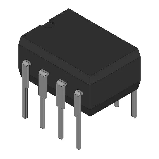
onsemi FOD3184TV — Optoisolators

onsemi FOD3184TV Gate Drive Optocoupler, 3A Peak, 8-DIP

MPNFOD3184TV
End of Life

onsemi FOD3184TV gate drive optocoupler, single-channel, 5000Vrms isolation, 3A peak output, 8-DIP through-hole package, Bulk.

$3.14Ref. price · indicative, final on quote
Packaging8-DIP (0.300", 7.62mm)
StockIn Stock (24)
Lead timeIn Stock wk
MOQ1 pcs
  • 100% new & originalTraceable channels only — no refurbs, no pulls, no remarked parts.
  • Date & lot codes on quoteStated per line before you commit; label photos on request.
  • MSL-compliant ESD packingMoisture-sealed bags with indicator cards; reels photo-verified.
  • PayPal buyer protectionPay by T/T, PayPal or Payoneer — card payments covered end to end.

Specifications

FOD3184TV Technical Specifications
ParameterValue
Mounting typeThrough Hole
Voltage - isolation5000Vrms
Voltage - output supply15V ~ 30V
Voltage - forward (Vf)1.43V
Current - peak output3A
Current - output high, low2.5A, 2.5A
Current - DC forward (If)25 mA
Operating temperature-40°C ~ 100°C
Pulse width distortion65ns
Approval agencyIEC/EN/DIN, UL
PackageBulk
TechnologyOptical Coupling
Case8-DIP (0.300\", 7.62mm)
Number of channels1
Rise (Fall time)38ns, 24ns
Propagation delay tpLH (tpHL)210ns, 210ns
Common mode transient immunity35kV/µs

Product details

3 A peak gate drive with 5 kV isolation

The onsemi FOD3184TV is a single-channel gate drive optocoupler delivering 3 A peak output current across a 5000 Vrms isolation barrier. This combination suits it for driving IGBTs and MOSFETs in motor drives, inverters, and industrial power supplies where the control side must float cleanly from the high-voltage bus. The 35 kV/µs minimum common-mode transient immunity means the output stays latched in its correct state when the bus voltage slews during a hard-switching event — a figure that matters for inverter legs switching at 10–20 kHz where the dV/dt at the collector can couple back through the parasitic capacitance of the optocoupler.

Switching speed and timing budget

Propagation delay is 210 ns max for both low-to-high and high-to-low transitions, with a pulse-width distortion ceiling of 65 ns. The 38 ns typical rise and 24 ns fall times keep the gate drive edges clean enough for most IGBT modules without external booster stages. The output stage sources and sinks 2.5 A symmetrically, which matches the peak rating of 3 A for the initial gate charge spike. The 15 V to 30 V output supply range covers standard gate drive rails — 15 V for IGBTs, 18 V for some MOSFETs, and 24 V for modules that need a higher gate overdrive.

Package and temperature grade

Housed in an 8-DIP through-hole package (0.300-inch body width), the FOD3184TV suits boards where wave solder is the primary assembly method. Approved under IEC/EN/DIN and UL — the UL recognition covers the 5000 Vrms isolation rating for reinforced insulation in mains-connected equipment.

Frequently asked questions

What is the peak output current of the FOD3184TV?

The FOD3184TV delivers 3 A peak output current, with a symmetrical 2.5 A high/low drive capability. This is sufficient to drive the gate charge of medium-power IGBTs and MOSFETs in a single switching cycle.

What isolation voltage does the FOD3184TV provide?

The FOD3184TV provides 5000 Vrms isolation between input and output, certified under IEC/EN/DIN and UL standards. This reinforced insulation rating suits it for applications requiring galvanic isolation between control and power stages.