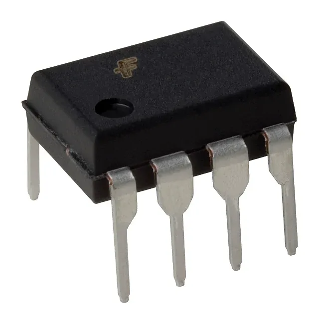
What the FOD3182V does in your power stage
The FOD3182V is a single-channel optoisolated gate driver from onsemi, built to drive IGBTs and power MOSFETs in motor drives, industrial inverters, and switched-mode power supplies. Its 3 A peak output current directly charges the gate capacitance of medium-power switches without an external booster stage. Reinforced isolation of 5000 Vrms meets the safety spacing requirements for motor-drive and industrial PSU designs, where the control side must be galvanically separated from the high-voltage DC bus. Common-mode transient immunity of 35 kV/µs minimum keeps the output state stable when the high-side switch sees fast dv/dt events — a common failure mode in half-bridge and three-phase inverter stages that can cause shoot-through if the driver falsely triggers.
Switching speed and timing margin
The 210 ns max propagation delay is symmetric between tpLH and tpHL, which simplifies dead-time calculation in complementary switching stages. Maximum pulse-width distortion of 65 ns means the on-time pulse width at the output stays within 65 ns of the input pulse width — a key parameter for applications like resonant converters where precise duty-cycle control matters.
Supply range and drive current
Output supply voltage spans 10 V to 30 V, covering the typical gate-drive levels for IGBTs (15 V) and MOSFETs (10–12 V) with margin. The 2.5 A source and sink current capability handles the peak gate charge of switches up to the 100 nC range at moderate switching frequencies. Forward voltage of 1.43 V typical at 25 mA max input current means the LED side can be driven directly from a 3.3 V or 5 V logic output with a series resistor — no extra level shifter needed on the control side.
Lifecycle, compliance, and package availability
Supplied in Tube, through-hole 8-DIP package. The 0.300-inch (7.62 mm) body width fits standard DIP sockets and breadboards, making it a practical choice for prototype builds and low-volume production where SMD reflow is not justified. Approved by UL and VDE — the dual-agency listing simplifies safety certification for equipment sold in North America and Europe.