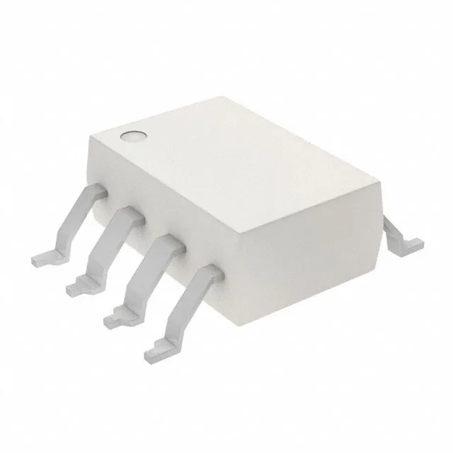
Gate driver with 3 A peak and 5 kV isolation
The FOD3182TSR2V is an onsemi single-channel optocoupled gate driver delivering 3 A peak output current across a 10 V to 30 V output supply range. The 5000 Vrms isolation rating and 35 kV/µs common-mode transient immunity make it suited for driving IGBTs and power MOSFETs in motor drives, inverters, and switch-mode power supplies where the high-side gate reference bounces at the switching node. Pulse width distortion is held to 65 ns max, which keeps the on-time symmetry tight enough for dead-time management in half-bridge and full-bridge topologies.
What the 3 A peak output means for your gate drive
The 3 A peak output is the current the driver can source or sink into the gate capacitance during the switching transient. For a typical IGBT with 100 nC total gate charge, the 38 ns rise time translates to a charging current of about 2.6 A — within the peak rating. The continuous output high/low current is 2.5 A, so the part can sustain moderate-frequency switching without thermal stress at the output stage. The 1.43 V typical forward voltage at 25 mA max input current means the LED side can be driven directly from a 3.3 V or 5 V logic output through a series resistor — no extra level shifter needed for the input side.
Package and footprint — 8-SMD Gull Wing
The 8-SMD Gull Wing package occupies the same PCB footprint as the through-hole FOD3182TV but requires a reflow profile instead of wave solder. The gull-wing leads are coplanar within 0.10 mm typical; the 1.27 mm pitch is layout-friendly on two-layer boards. The UL and VDE approval agency markings simplify safety certification for end equipment.