What this gate-drive optocoupler does for your power stage
The FOD3182SD is a single-channel optocoupled gate driver from onsemi, designed to drive IGBTs and power MOSFETs with a 3 A peak output current and 2.5 A symmetrical sink/source capability. Its 5 kVrms isolation rating provides the galvanic barrier needed between the low-voltage controller side and the high-voltage power stage, meeting UL approval for motor drives, inverters, and switch-mode power supplies. The 35 kV/µs minimum common-mode transient immunity means the output stays latched correctly when the power-stage midpoint slews at tens of kilovolts per microsecond — a common failure point in hard-switched bridges.
Switching speed and timing margin for your gate loop
Maximum propagation delay is 210 ns for both low-to-high and high-to-low transitions, with a pulse-width distortion of 65 ns max — a tight window that simplifies dead-time budgeting in complementary-switch topologies. The output supply range of 10 V to 30 V covers standard gate-drive rails for silicon IGBTs (15 V) and super-junction MOSFETs (12 V), while the 25 mA maximum forward current keeps the LED drive within a logic-level GPIO output range.
Package and temperature — what to check before the reflow oven
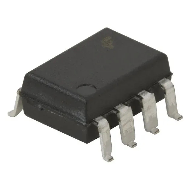
Housed in an 8-SMD Gull Wing package, the FOD3182SD has a standard 1.27 mm pitch footprint — no fine-pitch challenge for standard solder paste stencils, but check the MSL level on the reel label before reflow to avoid popcorning.