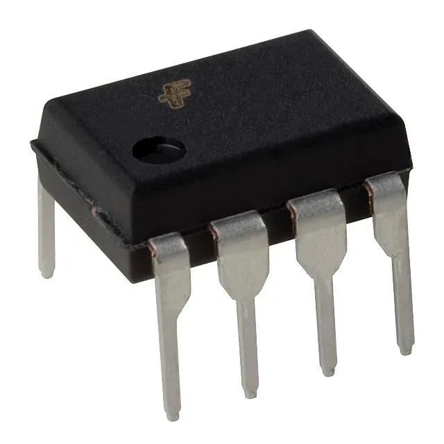
onsemi FOD3182 — Optoisolators

FOD3182 onsemi Optoisolator Gate Driver – 3A Peak, 5000Vrms

MPNFOD3182
End of Life

onsemi FOD3182, single-channel optocoupled gate driver, 5000Vrms isolation, 3A peak output, 8-DIP through-hole package, -40°C to 100°C operating range.

$3.16Ref. price · indicative, final on quote
Packaging8-DIP (0.300", 7.62mm)
StockContact for availability
MOQ1 pcs
  • 100% new & originalTraceable channels only — no refurbs, no pulls, no remarked parts.
  • Date & lot codes on quoteStated per line before you commit; label photos on request.
  • MSL-compliant ESD packingMoisture-sealed bags with indicator cards; reels photo-verified.
  • PayPal buyer protectionPay by T/T, PayPal or Payoneer — card payments covered end to end.

Specifications

FOD3182 Technical Specifications
ParameterValue
Mounting typeThrough Hole
Voltage - isolation5000Vrms
Voltage - output supply10V ~ 30V
Voltage - forward (Vf)1.43V
Current - peak output3A
Current - output high, low2.5A, 2.5A
Current - DC forward (If)25 mA
Operating temperature-40°C ~ 100°C
Pulse width distortion65ns
Approval agencyUL
PackageTube
TechnologyOptical Coupling
Case8-DIP (0.300\", 7.62mm)
Number of channels1
Rise (Fall time)38ns, 24ns
Propagation delay tpLH (tpHL)210ns, 210ns
Common mode transient immunity35kV/µs

Product details

Gate-driver optocoupler with 3 A peak and 5 kV isolation

The FOD3182 is an onsemi single-channel optocoupled gate driver delivering 3 A peak output current with 5000 Vrms isolation in an 8-DIP through-hole package. The 35 kV/µs minimum common-mode transient immunity keeps the output state stable during fast switching edges on the high-voltage side — a common failure point in motor-drive and inverter designs where the IGBT collector swings hundreds of volts in tens of nanoseconds. Rise and fall times are 38 ns and 24 ns typical, with a maximum propagation delay of 210 ns and pulse-width distortion held to 65 ns. The output supply range is 10 V to 30 V, covering standard gate-drive rails for IGBTs and power MOSFETs. Forward voltage is 1.43 V typical with a maximum DC forward current of 25 mA.

What the key ratings mean for your gate-drive design

The 3 A peak output is the current available to charge the IGBT or MOSFET gate capacitance during turn-on. For a typical 50 nC gate charge, the rise time into the gate is roughly 17 ns — fast enough for switching frequencies up to 100 kHz in hard-switched topologies. The 2.5 A high/low sourcing and sinking capability is symmetrical, so turn-off is equally fast, reducing dead-time requirements. 5000 Vrms isolation meets reinforced insulation requirements per UL for mains-connected industrial drives and power supplies. The 35 kV/µs minimum CMTI ensures the output does not glitch when the IGBT collector voltage slews rapidly — a spec that matters more than isolation voltage in noisy switching environments. The 8-DIP package is a through-hole footprint — expect a 0.100-inch pitch, 0.300-inch body width, compatible with standard DIP sockets or soldered directly into plated through-holes on a single-sided or double-sided PCB.

Frequently asked questions

Is FOD3182 a direct replacement for TLP250?

The FOD3182 and TLP250 are both single-channel optocoupled gate drivers in 8-DIP packages, but they are not pin-compatible drop-in replacements. Verify the pinout from the respective datasheets before substituting. The FOD3182 offers 3 A peak output compared to the TLP250's typical 1.5 A, so it can drive larger gate charges. Isolation voltage and CMTI also differ — check your application requirements.