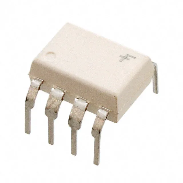
onsemi FOD3180TV — Optoisolators

onsemi FOD3180TV Optocoupler Gate Driver, 2.5A, 5000Vrms

MPNFOD3180TV
End of Life

onsemi FOD3180TV optocoupler gate driver, 1-channel, 2.5A peak output, 5000Vrms isolation, 15kV/µs CMTI, 8-DIP through-hole package, Tube.

$3.07Ref. price · indicative, final on quote
Packaging8-DIP (0.400", 10.16mm)
StockIn Stock (17)
Lead timeIn Stock wk
MOQ1 pcs
  • 100% new & originalTraceable channels only — no refurbs, no pulls, no remarked parts.
  • Date & lot codes on quoteStated per line before you commit; label photos on request.
  • MSL-compliant ESD packingMoisture-sealed bags with indicator cards; reels photo-verified.
  • PayPal buyer protectionPay by T/T, PayPal or Payoneer — card payments covered end to end.

Specifications

FOD3180TV Technical Specifications
ParameterValue
Mounting typeThrough Hole
Voltage - isolation5000Vrms
Voltage - output supply10V ~ 20V
Voltage - forward (Vf)1.43V
Current - peak output2.5A
Current - output high, low2A, 2A
Current - DC forward (If)25 mA
Operating temperature-40°C ~ 100°C
Pulse width distortion65ns
Approval agencycUL, UL, VDE
PackageTube
TechnologyOptical Coupling
Case8-DIP (0.400\", 10.16mm)
Number of channels1
Rise (Fall time)75ns, 55ns
Propagation delay tpLH (tpHL)200ns, 200ns
Common mode transient immunity15kV/µs

Product details

Gate-drive isolation for inverter and motor-drive stages

The onsemi FOD3180TV is a 1-channel optocoupler gate driver delivering 2.5 A peak output current with 5000 Vrms isolation — enough to drive the gate charge of a standard IGBT or power MOSFET in a motor-drive or UPS inverter leg without a separate booster stage.

Switching speed and timing symmetry

Rise and fall times of 75 ns and 55 ns typical, with propagation delays of 200 ns max — the 65 ns max pulse-width distortion keeps the on/off timing symmetric, so the dead-time budget in a half-bridge doesn't need to absorb asymmetric delays. The 2 A source and 2 A sink capability means the gate charges and discharges at the same rate, avoiding slow turn-off that could push the switch into the linear region during hard switching. Common-mode transient immunity of 15 kV/µs minimum ensures the output doesn't glitch when the high-side switch's source node slews at inverter switching frequencies — a spec that matters more than raw isolation voltage in a noisy drive environment.

The output supply range of 10 V to 20 V covers standard IGBT gate thresholds (typically 12 V to 15 V) and leaves headroom for desaturation detection circuits that pull the gate low during fault.

Housed in an 8-DIP (0.400", 10.16 mm) through-hole package with the 8-MDIP supplier device code — the wider 0.400" body gives 8 mm creepage between input and output pins, helping meet reinforced-insulation spacing on a two-layer board. Supplied in Tube packaging — expected for through-hole DIPs; no tape-and-reel option, so pick-and-place requires a tube feeder or manual insertion.

Compliance and lifecycle posture

Approved by cUL, UL, and VDE — the VDE mark is the key one for European machinery directives; UL recognition covers North American panel builds.

Frequently asked questions

What is the closest pin-compatible alternative to FOD3180TV?

The part is sourced as the sole listed variant; any alternative would require a board-level comparison of pinout, isolation rating, and output drive strength.

What compliance documentation does onsemi provide for FOD3180TV?

The part carries cUL, UL, and VDE approvals and is ROHS3 compliant. UL file and VDE certificate numbers are typically printed on the device label or available through onsemi's compliance portal.