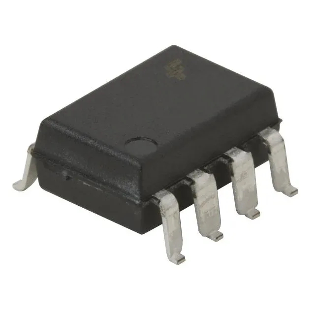
onsemi FOD3150ASD — Optoisolators

FOD3150ASD Optoisolated Gate Driver – 5000 Vrms, 3 A Peak

MPNFOD3150ASD
End of Life

onsemi FOD3150ASD, single-channel optoisolated gate driver, 5000 Vrms isolation, 3 A peak output, 60 ns rise/fall, 8-SMD gull wing, -40°C to 100°C

$1.98Ref. price · indicative, final on quote
Packaging8-SMD, Gull Wing
StockContact for availability
MOQ1 pcs
  • 100% new & originalTraceable channels only — no refurbs, no pulls, no remarked parts.
  • Date & lot codes on quoteStated per line before you commit; label photos on request.
  • MSL-compliant ESD packingMoisture-sealed bags with indicator cards; reels photo-verified.
  • PayPal buyer protectionPay by T/T, PayPal or Payoneer — card payments covered end to end.

Specifications

FOD3150ASD Technical Specifications
ParameterValue
Mounting typeSurface Mount
Voltage - isolation5000Vrms
Voltage - output supply15V ~ 30V
Voltage - forward (Vf)1.5V
Current - peak output3A
Current - output high, low2A, 2A
Current - DC forward (If)25 mA
Operating temperature-40°C ~ 100°C
Pulse width distortion300ns
Approval agencyUL
PackageTape & Reel (TR); Cut Tape (CT)
TechnologyOptical Coupling
Case8-SMD, Gull Wing
Number of channels1
Rise (Fall time)60ns, 60ns
Propagation delay tpLH (tpHL)500ns, 500ns
Common mode transient immunity20kV/µs

Product details

Gate-drive isolation for 600–1200 V inverter legs

The FOD3150ASD is a single-channel optoisolated gate driver rated for 5000 Vrms isolation. The 3 A peak output drives the gate charge of medium-power IGBTs and MOSFETs, turning them on in 60 ns typical. Its common-mode transient immunity of 20 kV/µs minimum keeps the output state stable when the high-side switch sees a fast voltage step across the isolation barrier — a common failure mode in half-bridge and H-bridge topologies.

Parametric deep-dive: timing and drive strength

Propagation delay is 500 ns max for both tpLH and tpHL, with pulse-width distortion held to 300 ns max. These numbers set the dead-time margin in a phase-leg: a 500 ns propagation delay means the complementary gate signal must be delayed by at least that much plus the 300 ns distortion to avoid shoot-through. Output high/low current is 2 A each, symmetrical. The output supply range of 15 V to 30 V covers standard IGBT gate drive voltages. The LED forward voltage is 1.5 V typical, and the maximum forward current is 25 mA.

Lifecycle and sourcing status

ROHS3 compliant. The 8-SMD gull-wing package is supplied in Tape & Reel or Cut Tape, which keeps it compatible with standard pick-and-place lines. No stock-holding claim; we quote to order.

Package fit and board layout

8-SMD gull-wing package. The 8-SMD supplier device package footprint matches standard SOIC-8 land patterns. Operating temperature range -40°C to 100°C covers industrial motor-drive cabinets, outdoor telecom shelters, and under-hood automotive auxiliary inverters. The UL approval simplifies system-level safety certification.

Frequently asked questions

What is the peak output current of FOD3150ASD?

3 A peak output. The high/low continuous output current is 2 A each, so the peak rating handles the initial gate charge surge while the continuous rating supports the average gate drive current at the switching frequency.

What package is FOD3150ASD available in?

8-SMD gull wing, also listed as 8-SMD supplier device package. Supplied in Tape & Reel or Cut Tape. Surface-mount, 1.27 mm pitch, standard SOIC-8 footprint.

How does FOD3150ASD compare to the FOD3184SD?

The FOD3184SD offers faster switching — 38 ns rise, 24 ns fall vs 60 ns/60 ns — and higher CMTI at 35 kV/µs vs 20 kV/µs. Both have 3 A peak output and 5000 Vrms isolation. The FOD3184SD also carries VDE approval in addition to UL. If your design needs tighter dead-time margins or operates in a higher dv/dt environment, the FOD3184SD is a drop-in compatible upgrade in the same 8-SMD package.