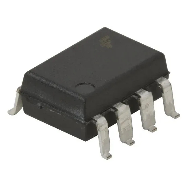
onsemi FOD3120SV — Optoisolators

onsemi FOD3120SV Optoisolator, 5 kV, 3 A Gate Driver, 8-SMD

MPNFOD3120SV
End of Life

onsemi FOD3120SV optoisolated gate driver, single-channel, 5000 Vrms isolation, 3 A peak output, 8-SMD gull-wing package, tube.

$2.0Ref. price · indicative, final on quote
Packaging8-SMD, Gull Wing
StockContact for availability
Lead timeIn Stock wk
MOQ1 pcs
  • 100% new & originalTraceable channels only — no refurbs, no pulls, no remarked parts.
  • Date & lot codes on quoteStated per line before you commit; label photos on request.
  • MSL-compliant ESD packingMoisture-sealed bags with indicator cards; reels photo-verified.
  • PayPal buyer protectionPay by T/T, PayPal or Payoneer — card payments covered end to end.

Specifications

FOD3120SV Technical Specifications
ParameterValue
Mounting typeSurface Mount
Voltage - isolation5000Vrms
Voltage - output supply15V ~ 30V
Voltage - forward (Vf)1.5V
Current - peak output3A
Current - output high, low2A, 2A
Current - DC forward (If)25 mA
Operating temperature-40°C ~ 100°C
Pulse width distortion100ns
Approval agencyIEC, UL
PackageTube
TechnologyOptical Coupling
Case8-SMD, Gull Wing
Number of channels1
Rise (Fall time)60ns, 60ns
Propagation delay tpLH (tpHL)400ns, 400ns
Common mode transient immunity35kV/µs

Product details

Gate-driver optocoupler for IGBT/MOSFET switching

The onsemi FOD3120SV is a single-channel optoisolated gate driver delivering 3 A peak output current with 5000 Vrms isolation, sized for driving IGBTs and power MOSFETs in motor drives, inverters, and industrial power supplies. The 35 kV/µs minimum common-mode transient immunity (CMTI) means the output stays latched to the correct state when the high-side switch node slews at tens of kV/µs — a key spec for half-bridge topologies where dv/dt couples across the isolation barrier.

Switching speed and timing margin

Propagation delay is 400 ns max (tpLH and tpHL) with a 100 ns max pulse-width distortion — the delay mismatch between turn-on and turn-off is tight enough to avoid dead-time errors in complementary switching stages. Rise and fall times are 60 ns typical each, so the gate drive edge is clean for switching frequencies up to the mid-hundreds of kHz without excessive cross-conduction.

Supply range and output drive strength

The output supply rail spans 15 V to 30 V, covering the standard gate-drive voltages for IGBTs (15 V on, -5 V to -15 V off) and MOSFETs (10 V to 12 V logic-level, 15 V standard). Peak output current is 3 A, with 2 A source and 2 A sink capability — enough to charge and discharge the gate capacitance of a medium-power IGBT module in under 200 ns.

Temperature range and approvals

Approved to IEC and UL standards, and ROHS3 compliant — the component is accepted in equipment shipped to European and North American markets without additional certification cost.

Frequently asked questions

Where can I buy FOD3120SV and how do I get a price?

The FOD3120SV is sourced through independent distribution. Submit an RFQ for current availability and pricing — the quote is confirmed at order time.

What compliance documentation does onsemi provide for FOD3120SV?

The FOD3120SV is ROHS3 compliant and carries IEC and UL approvals. Standard compliance documentation is available on request.