Obsolete — sourcing for existing BOM lines
The CNY17F1TM is officially listed as Obsolete by onsemi. For designs already using this part, independent distribution channels hold inventory.
Rated for 4170 Vrms isolation between input and output — this is the withstand voltage for reinforced insulation in a 250 V working-voltage system. The 1-channel DC-input transistor output is a standard phototransistor optocoupler topology. Current transfer ratio (CTR) is specified at 40% min and 80% max, measured at If=10 mA. This binning means the gain is tightly controlled — a design that expects at least 40% CTR at 10 mA forward current will not see a weak unit that fails to pull the output low. Switching speed is characterised by turn-on time of 2 µs typ and turn-off time of 3 µs typ, with rise/fall times of 4 µs / 3.5 µs max. For a 10 kHz PWM signal, the 3 µs turn-off delay eats about 3% of the period — fine for status feedback, marginal for high-speed isolation gates.
Package and temperature grade
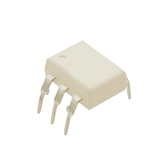
Housed in a 6-DIP through-hole package (0.400-inch lead spacing, 10.16 mm body width), the CNY17F1TM mates with standard 0.100-inch pitch sockets or solder holes. Output rating: 70 V collector-emitter max, 50 mA continuous output current. The 400 mV Vce(sat) at rated current means the output transistor saturates cleanly for TTL or 5 V logic interfaces.