Isolation barrier and key parametrics
The CNY17F13SD: This isolation rating qualifies it for reinforced insulation in mains-referenced circuits — enough for line-voltage sensing, SMPS feedback, or PLC digital input isolation where the working voltage stays below 250Vrms. Current transfer ratio (CTR) is specified at 40% minimum and 80% maximum, measured at 10mA forward current. This binning guarantees the phototransistor will switch on within a known gain window — critical when the downstream logic threshold is fixed and the LED drive current is already set by the BOM resistor.
Switching speed and output drive
Typical turn-on time is 2µs and turn-off time is 3µs, with rise and fall times of 1µs and 2µs respectively. For a 10kHz PWM signal, the 3µs turn-off delay eats about 3% of the period — acceptable for status feedback or relay drive, but too slow for high-speed serial isolation or gate-drive applications. The output transistor can sink up to 50mA continuous at a maximum collector-emitter voltage of 70V. Vce(sat) is clamped at 300mV, so the voltage drop across the output at full load stays under a third of a volt — useful when driving a 5V logic input directly without a pull-up resistor.
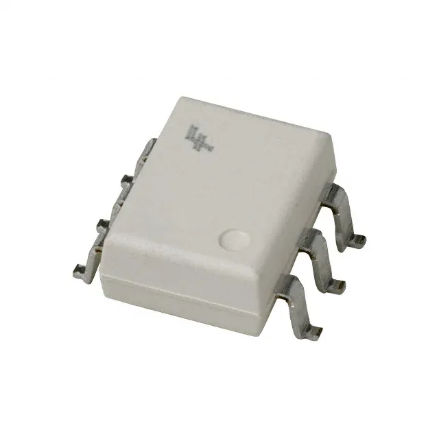
Housed in a 6-pin SMD gull-wing package (6-SMD), the CNY17F13SD occupies the same footprint as the standard DIP-6 through-hole optoisolator but with a surface-mount body. The gull-wing leads provide a visible solder joint for AOI inspection and the 6-SMD supplier device package designation matches the standard SOIC-6 wide-body land pattern. Rated for operation from -55°C to +100°C, the part covers industrial temperature ranges including cold-start environments. The tape-and-reel packaging (TR suffix) is ready for automated pick-and-place assembly.
Lifecycle reality
onsemi has marked the CNY17F13SD as Obsolete.