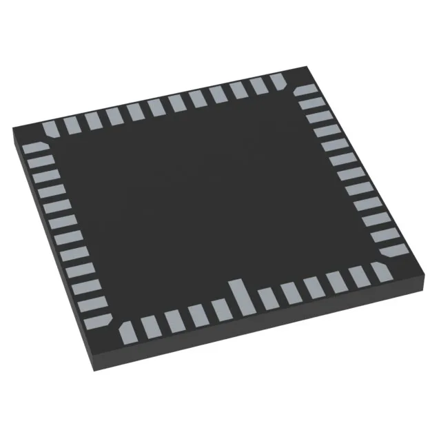
1.2 MP mono imager with on-chip ISP
The onsemi AR0134CSSM00SPCA0-DRBR is a 1/3-inch format CMOS image sensor with an integrated image signal processor, outputting processed monochrome frames at 1280H x 960V resolution. The 3.75 µm pixel pitch gives it a per-pixel light collection area roughly 2.5× larger than a 2.2 µm pixel, so low-light sensitivity is higher — a meaningful advantage for surveillance or machine-vision cameras that must capture usable images at 0.1 lux or below. Runs from a single 1.7 V supply rail, which simplifies the power tree — no separate analog or I/O voltage domain is required. The sensor is rated for -30°C to 70°C ambient, covering most indoor and outdoor security, industrial inspection, and traffic-camera enclosures.
Frame rate and pixel architecture
At full 1280H x 960V resolution the sensor delivers 54 FPS. This frame rate is set by the pixel array readout timing and the on-chip ADC conversion rate; it is the maximum rate at which the sensor can output full-resolution frames without subsampling or binning. For applications that need higher temporal resolution (e.g., 100+ FPS), the sensor supports windowed readout — cropping the active area reduces the row count and increases the achievable frame rate proportionally. The 3.75 µm pixel uses a 4T (four-transistor) pinned-photodiode architecture, which keeps dark current low and supports correlated double sampling for reduced read noise. This matters for applications where signal-to-noise ratio at low light is the limiting factor — the larger pixel collects more photons per integration period than a smaller pixel would at the same f-number.
The part is still a valid BOM line for new designs and production builds. The sensor ships in a JEDEC tray (not tape-and-reel). For high-volume pick-and-place lines that require reel feed, the sibling order code AR0134CSSC00SUEA0-TPBR is the tape-and-reel variant with the same die, pixel array, and frame rate.