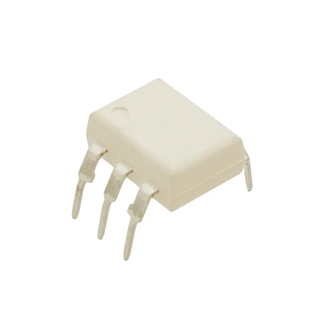
The 4N37W is listed as obsolete by onsemi. Sourcing runs through independent distribution — quantities and lead time confirmed at RFQ against your BOM line.
5300Vrms isolation and the safety barrier it buys
Rated for 5300Vrms isolation, this optocoupler provides a reinforced insulation barrier between the input LED and output phototransistor. That figure qualifies it for mains-referenced circuits where the creepage and clearance across the 6-DIP body must hold off transient overvoltages per IEC 60950-1 or IEC 62368-1 — think AC-line monitoring, motor-drive feedback, or industrial PSU secondary-side sensing. At lower drive currents the CTR drops; budget the 10 mA figure into your LED resistor calculation. Switching is rated at 2 µs turn-on and 2 µs turn-off typical. That 4 µs total propagation suits logic-level signals up to about 100 kHz — plenty for isolated serial data, PLC input debounce, or gate-drive fault feedback. For faster edges the transistor-with-base output lets you add a speed-up capacitor between base and emitter to reduce storage time.
Through-hole 6-DIP — legacy board fit
The 6-DIP (0.400-inch, 10.16 mm) through-hole package is the standard optocoupler footprint for hand-assembled or wave-soldered boards. The 300 mV maximum Vce saturation at the output means the phototransistor pulls down to within 300 mV of the emitter rail — clean logic-low for TTL or CMOS inputs. The 100 mA absolute-maximum forward current on the LED side sets the ceiling for the input resistor; running at 10–20 mA keeps the LED junction well below its stress limit. Operating temperature spans -55°C to 100°C — the full industrial range. The 1.18 V typical forward voltage at 10 mA is the drop to use for input power dissipation calculations.