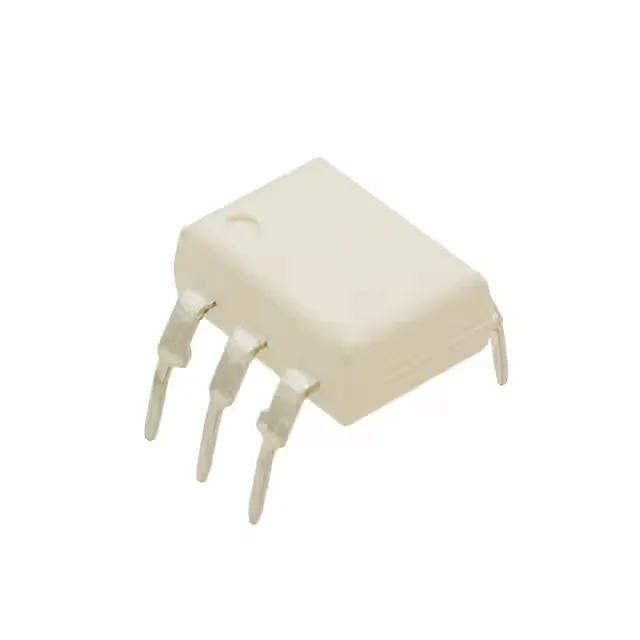
What the 5300Vrms isolation means on the bench
The 4N25300W: The 5300Vrms isolation rating means it safely separates a low-voltage control side from a higher-voltage power side — think PLC digital inputs, motor drive feedback, or any signal crossing a safety barrier where a direct connection would risk ground loops or shock. The base terminal on the output side lets you bias the transistor for faster switching or higher gain — useful when the downstream logic needs a clean edge. The 2µs turn-on and turn-off times are typical for this generation of phototransistor isolators; fast enough for 10-100 kHz signal isolation but not for high-speed data links.
Lifecycle reality — obsolete, but findable
onsemi lists the 4N25300W as obsolete. For a field swap or a repair run, the 4N25 family is widely second-sourced. A pin-compatible alternative from another brand with the same 6-DIP footprint and 5300Vrms isolation can often drop in without a board spin, but the CTR bin and base-bias behaviour should be checked against the original spec.
What the key ratings drive in a BOM
The 20% minimum current transfer ratio at 10 mA forward current sets the LED drive requirement — you need at least 10 mA through the input LED to guarantee the output transistor pulls its collector low. The output transistor is rated for 30V collector-emitter maximum and saturates at 500mV — fine for 5V and 24V logic families. The 100 mA maximum forward current on the input side gives headroom for noisy environments where you might overdrive the LED to guarantee turn-on. The -55°C to 100°C operating range covers industrial and some military-temperature applications — the phototransistor leakage doubles roughly every 10°C, so at the high end the off-state collector current needs to be checked against the load impedance.
The tube packaging means the parts come aligned for auto-insertion or hand-stuffing. No lab, no bench — this is a socket-friendly part. The pinout is standard for the 4N25 family: pin 1 is the LED anode, pin 2 the cathode, pin 5 the transistor collector, pin 4 the emitter, and pin 6 the base. Orientation is obvious from the notch at pin 1 end.