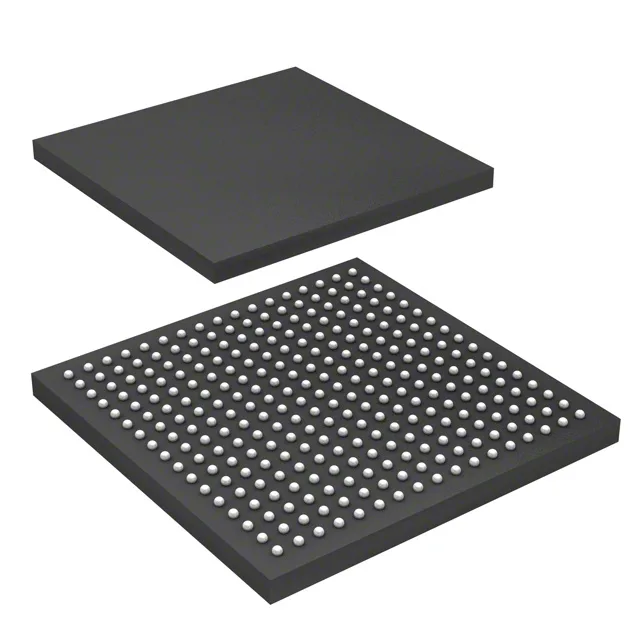
NXP Semiconductors MCIMX6Y2CVM08AB — Microcontrollers & Processors (MCU / MPU / DSP)

NXP MCIMX6Y2CVM08AB i.MX6 MPU, 792MHz, 289-MAPBGA

MPNMCIMX6Y2CVM08AB
End of Life

NXP Semiconductors i.MX6 series application processor, MCIMX6Y2CVM08AB, ARM Cortex-A7 single-core 792 MHz, 289-MAPBGA (14x14 mm), -40 to +105 °C, dual USB 2.0 OTG + PHY, dual 10/100 Ethernet.

$17.65Ref. price · indicative, final on quote
Packaging289-LFBGA
StockContact for availability
MOQ1 pcs
  • 100% new & originalTraceable channels only — no refurbs, no pulls, no remarked parts.
  • Date & lot codes on quoteStated per line before you commit; label photos on request.
  • MSL-compliant ESD packingMoisture-sealed bags with indicator cards; reels photo-verified.
  • PayPal buyer protectionPay by T/T, PayPal or Payoneer — card payments covered end to end.

Specifications

MCIMX6Y2CVM08AB Technical Specifications
ParameterValue
Seriesi.MX6
Mounting typeSurface Mount
Voltage - i (O)1.8V, 2.8V, 3.3V
Additional interfacesCANbus, I²C, SPI, UART
Display & interface controllersElectrophoretic, LCD
Operating temperature-40°C ~ 105°C (TJ)
Number of cores (Bus width)1 Core, 32-Bit
USBUSB 2.0 OTG + PHY (2)
Speed792MHz
PackageTray
Ethernet10/100Mbps (2)
Core processorARM® Cortex®-A7
Case289-LFBGA
RAM controllersLPDDR2, DDR3, DDR3L
Co-Processors (DSP)Multimedia; NEON™ MPE
Security featuresA-HAB, ARM TZ, CSU, SJC, SNVS
Graphics accelerationNo

Product details

792 MHz Cortex-A7 with industrial temperature range

The MCIMX6Y2CVM08AB is a single-core ARM Cortex-A7 application processor from the NXP i.MX6 series, clocked at 792 MHz. This speed grade, combined with the -40 to +105 °C junction temperature rating, fits cost-optimized Linux or RTOS designs in factory automation, HMI, and IoT gateway applications where the ambient exceeds commercial limits.

Memory interface and peripheral set for industrial connectivity

The memory controller supports LPDDR2, DDR3, and DDR3L, giving the BOM engineer flexibility to trade cost against bandwidth — DDR3L at 1.35 V reduces system power in thermally constrained enclosures. Two USB 2.0 OTG interfaces with integrated PHY eliminate external USB transceivers, while the dual 10/100 Ethernet MACs enable a dual-network gateway or a daisy-chain topology without an external switch IC. Additional wired interfaces include CANbus, I²C, SPI, and UART — the CAN controller covers industrial fieldbus bridging, and the I²C/SPI count supports sensor and display peripheral expansion.

Security features and display support

The security subsystem includes A-HAB (Advanced High-Assurance Boot), ARM TrustZone, CSU (Central Security Unit), SJC (Secure JTAG Controller), and SNVS (Secure Non-Volatile Storage). This qualifies the part for secure-boot chains and trusted-execution environments in payment terminals or access-control panels. Display and interface controllers support electrophoretic (E Ink) and LCD panels — relevant for low-power signage or industrial HMI where the display refresh rate is modest. The NEON MPE coprocessor provides single-instruction multiple-data (SIMD) acceleration for multimedia and signal-processing tasks, though there is no dedicated graphics accelerator.

Package, supply rails, and compliance

Housed in a 289-ball MAPBGA measuring 14x14 mm with a 0.8 mm ball pitch.

Frequently asked questions

What is MCIMX6Y2CVM08AB's listed speed and USB interface?

The core processor runs at 792 MHz. The part integrates two USB 2.0 OTG interfaces with on-chip PHY, eliminating the need for external USB transceivers in dual-role host/device designs.

What memory types does the MCIMX6Y2CVM08AB support?

The memory controller supports LPDDR2, DDR3, and DDR3L. This allows the BOM engineer to select the memory technology that best balances cost, speed, and power — DDR3L at 1.35 V is the lower-power option for thermally constrained enclosures.