The ARM Cortex-A9 core with NEON SIMD engine provides enough integer and signal-processing throughput for 2D graphics compositing, basic computer-vision pre-processing, and control-loop tasks without needing a separate DSP. The 1.0 GHz clock gives headroom for Linux or RTOS-based stacks running lightweight GUI frameworks. Three USB 2.0 ports with integrated PHY cover host and OTG roles — enough for a keyboard, a touch controller, and a USB storage device or cellular modem. The single 10/100 Ethernet MAC connects to a PHY for wired networking, though the part lacks a built-in switch, so multi-port designs need an external switch IC. On-chip security includes ARM TrustZone, secure boot, cryptography acceleration, secure fuse box, secure JTAG, secure memory, secure RTC, and tamper detection. This qualifies the MCIMX6L2EVN10AB for payment terminals, access-control panels, and any edge device that must resist physical or software attacks. The 1.2V, 1.8V, and 3.0V I/O voltage rails simplify interfacing to both low-voltage memory and legacy 3.0V peripherals.
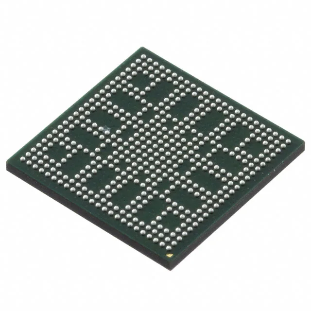
NXP MCIMX6L2EVN10AB i.MX6SL ARM Cortex-A9 MPU, 1.0 GHz
NXP i.MX6SL series, MCIMX6L2EVN10AB, ARM Cortex-A9 MPU, 1.0 GHz, 1 Core, 32-Bit, LPDDR2/LVDDR3/DDR3, USB 2.0 + PHY (3), 10/100Mbps Ethernet, -40°C ~ 105°C, 432-MAPBGA (13x13), Tray.
Specifications
| Parameter | Value |
|---|---|
| Series | i.MX6SL |
| Mounting | Surface Mount |
| Voltage - i (O) | 1.2V, 1.8V, 3.0V |
| Additional interfaces | AC97, I²C, I²S, MMC/SD/SDIO, SPI, SSI, UART |
| Display & interface controllers | Keypad, LCD |
| Operating temperature | -40°C ~ 105°C (TA) |
| Number of cores (Bus width) | 1 Core, 32-Bit |
| USB | USB 2.0 + PHY (3) |
| Speed | 1.0GHz |
| Package | Tray |
| Ethernet | 10/100Mbps (1) |
| Core processor | ARM® Cortex®-A9 |
| Case | 432-TFBGA |
| RAM controllers | LPDDR2, LVDDR3, DDR3 |
| Co-Processors (DSP) | Multimedia; NEON™ SIMD |
| Security features | ARM TZ, Boot Security, Cryptography, RTIC, Secure Fusebox, Secure JTAG, Secure Memory, Secure RTC, Tamper Detection |
| Graphics acceleration | Yes |
Product details
Frequently asked questions
What memory types does MCIMX6L2EVN10AB support?
The integrated memory controller supports LPDDR2, LVDDR3, and DDR3, giving the designer flexibility to choose the most cost-effective or power-efficient memory technology.
Is MCIMX6L2EVN10AB compatible with DDR3 memory?
Yes, DDR3 is one of the supported RAM controller interfaces, along with LPDDR2 and LVDDR3.
What is the difference between MCIMX6L2EVN10AB and MCIMX6L3EVN10AB?
The MCIMX6L3EVN10AB is a higher-tier member of the i.MX6SL family. The exact delta in core count, graphics, or peripheral set should be verified against the respective datasheets, but typically the variant adds more performance or connectivity headroom. For a pin-compatible drop-in, confirm the package and memory controller alignment.