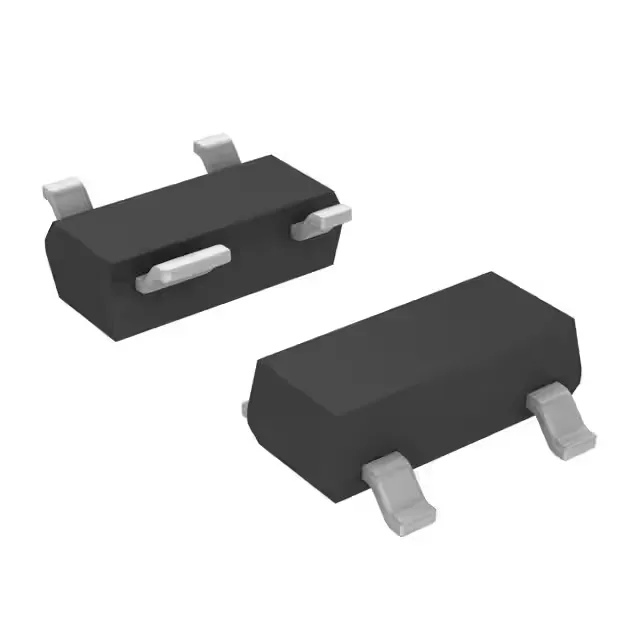
NXP Semiconductors BFU520XRR — Discrete Semiconductors

NXP BFU520XRR RF Transistor NPN, 10.5GHz, 20dB Gain

MPNBFU520XRR
End of Life

NXP Semiconductors BFU520XRR NPN RF transistor, 10.5 GHz transition frequency, 20 dB gain, 0.65 dB noise figure at 900 MHz, AEC-Q101 automotive qualified, SOT-143R surface mount package.

$0.47Ref. price · indicative, final on quote
PackagingSOT-143R
StockContact for availability
MOQ1 pcs
  • 100% new & originalTraceable channels only — no refurbs, no pulls, no remarked parts.
  • Date & lot codes on quoteStated per line before you commit; label photos on request.
  • MSL-compliant ESD packingMoisture-sealed bags with indicator cards; reels photo-verified.
  • PayPal buyer protectionPay by T/T, PayPal or Payoneer — card payments covered end to end.

Specifications

BFU520XRR Technical Specifications
ParameterValue
Mounting typeSurface Mount
FET typeNPN
Voltage - collector emitter breakdown12V
Current - collector (Ic)30mA
DC current gain (hFE) (Min) @ ic, vce60 @ 5mA, 8V
Power - max450mW
Frequency10.5GHz
Operating temperature-40°C ~ 150°C (TJ)
Gain20dB
GradeAutomotive
PackageTape & Reel (TR); Cut Tape (CT)
QualificationAEC-Q101
CaseSOT-143R
Noise figure (dB typ @ f)0.65dB @ 900MHz

Product details

RF performance for LNA and driver stages

The BFU520XRR is an NPN RF transistor from NXP, designed for low-noise amplification up to the low-GHz range. Its 10.5 GHz transition frequency and 20 dB gain make it suitable for LNA, driver, and buffer stages in automotive RF systems like tire-pressure monitoring, keyless entry, and telematics modules. The noise figure of 0.65 dB at 900 MHz is the figure of merit for front-end sensitivity — every tenth of a dB directly impacts the receiver's cascaded noise floor. For a 900 MHz ISM-band receiver, this transistor keeps the system NF below 1 dB with proper input matching.

Automotive-grade reliability and thermal envelope

Qualified to AEC-Q101, the BFU520XRR meets the stress, lifetime, and production-control requirements for automotive electronics. Maximum collector current is 30 mA with a collector-emitter breakdown of 12 V. These are the absolute-maximum ratings, not the bias point — the nominal operating region sits well below these limits. The 450 mW power dissipation in the SOT-143R package sets the thermal budget; for a typical LNA biased at 5 V and 10 mA, the 50 mW dissipation leaves ample margin.

SOT-143R footprint and board integration

The SOT-143R package is a four-lead surface-mount footprint with a collector pad that doubles as the thermal path. The PCB layout should follow the recommended land pattern in the NXP application note — the emitter leads are on opposite sides of the package, which simplifies the RF ground via placement for a common-emitter stage.

Frequently asked questions

What is the noise figure of BFU520XRR at 900 MHz?

The BFU520XRR has a typical noise figure of 0.65 dB at 900 MHz. This low NF makes it a strong candidate for the first LNA stage in a 900 MHz ISM-band receiver, where cascaded noise figure directly sets the system sensitivity.

What compliance documentation does NXP provide for BFU520XRR?

NXP provides the standard compliance declarations; specific REACH, UL, or IEC documentation should be requested through the supply chain at quote time.