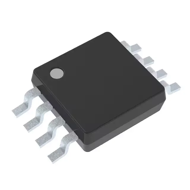
Active AEC-Q100 triple inverter for 5V automotive logic
The 74HCT3G04DP-Q100125: That means this part is certified for underhood or engine-bay deployment where the silicon sees sustained 105°C+ on a summer grade, not just cabin electronics. Three independent inverter gates in a single 8-TSSOP package, each with a 4mA symmetrical output drive at 5V supply. The 18ns max propagation delay at 4.5V into 50pF sets the data-rate ceiling for a 5V logic bus — adequate for ECU sensor interfaces running below 10 MHz, but not a high-speed clock tree.
Supply rails and quiescent discipline
Runs on a single 4.5V to 5.5V rail — a standard 5V automotive supply with ±10% margin covers the full operating range. The 1µA max quiescent current means this inverter adds negligible standby draw in a body-controller module that stays powered during key-off. Input logic thresholds are 0.8V low and 2.0V high at 5V VCC, compatible with 3.3V logic driving the inputs as long as the high-level output from the previous stage exceeds 2V. No level translation needed between a 3.3V MCU and this inverter when the MCU outputs 3.3V CMOS levels.
Surface-mount assembly with no exposed pad means the thermal path is through the leads only; the junction-to-ambient thermal resistance is adequate for the 4mA output current at 125°C ambient. Bulk packaging (tube or tray) is typical for engineering samples or low-volume production; for high-volume reels confirm the reel quantity with the distributor at RFQ. The part is RoHS-compliant per NXP's standard automotive grade, with full PPAP documentation available through the supply chain.