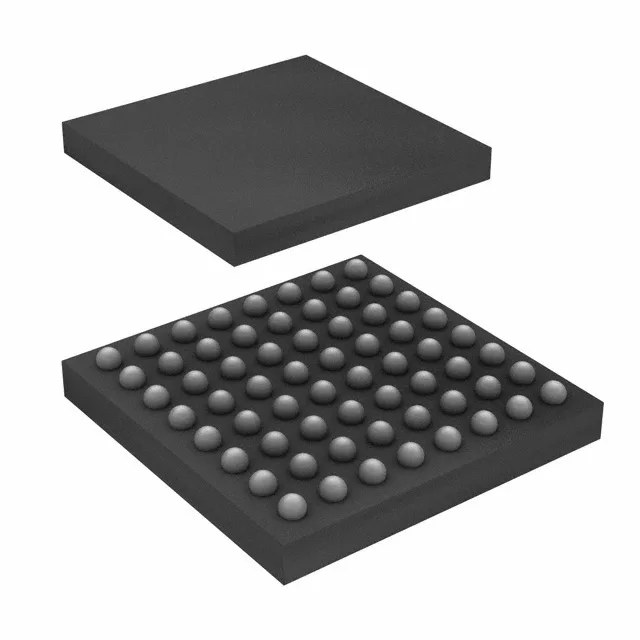
The NXP MKL81Z128CBH7R is a Kinetis KL8 series 32-bit ARM Cortex-M0+ MCU clocked at 72 MHz, with 128 KB Flash and 96 KB RAM. That RAM-to-Flash ratio is generous for this core class — enough headroom for USB OTG buffer pools or a small audio I²S stream without external SRAM. The 64-WLCSP package (3.48×3.38 mm) saves real estate on a dense mixed-signal board, but it's a wafer-level chip-scale part: plan for controlled reflow, X-ray inspection, and underfill if the assembly sees shock or vibration. Forty-one I/O in that footprint means most pads are dual-function; the pinout needs careful review before the layout freeze.
Rated -40 to 105 °C. The internal oscillator trims out the external crystal for many UART and I²C applications, but USB OTG still wants a precision clock source for bit-level timing.
Peripherals and connectivity — what's on the bus
The 11-channel 16-bit ADC and the 12-bit DAC handle analog front-end tasks; the 6-bit DAC is a smaller auxiliary channel. DMA, I²S, POR, LVD, PWM, and WDT round out the peripheral set. No CAN or Ethernet on this die — if you need those, step up to a Kinetis K or L series with the appropriate peripheral module.