Dual-core architecture for mixed-tasking control
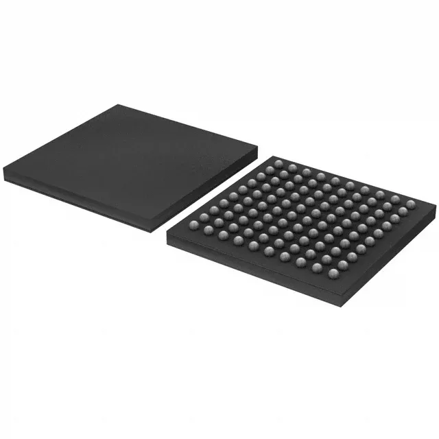
The NXP LPC4322JET100E runs a 32-bit ARM Cortex-M4 at 204 MHz for the main control loop, with a Cortex-M0 companion core that handles communications or low-power housekeeping without loading the M4. That split means you can keep a Modbus or CAN stack running on the M0 while the M4 processes sensor fusion or motor commutation — no interrupt thrash between tasks. Program memory is 512 KB of Flash, backed by 104K x 8 SRAM and a separate 16K x 8 EEPROM block for calibration constants or boot parameters that survive a firmware update. The EEPROM is a practical detail — saves an external serial EEPROM on the BOM if you need non-volatile trim values. The 100-TFBGA package (9x9 mm) keeps board area tight, but you'll want a solder profile that matches the fine-pitch BGA.
Peripherals include CANbus, USB with OTG, multiple SPI/I²C/UART interfaces, an external memory interface (EBI/EMI), and an I²S audio port. The EBI is worth noting if you need to hang an external SRAM or FPGA configuration memory off the bus — it saves a serial-to-parallel bridge. On-chip data converters: four 10-bit ADC channels and one 10-bit DAC. Not a high-resolution analog front-end, but adequate for current-sense feedback or simple analog output loops.