1:20 clock fanout with HCSL outputs
The ZL40292LDF1 is a 1:20 fanout buffer from Microchip Technology, designed to distribute a single differential clock input to twenty HCSL (High-Speed Current Steering Logic) outputs. The part handles clock frequencies up to 250 MHz and operates from a 3.135 V to 3.465 V supply rail. The 1:20 ratio means a single clock source fans out to twenty independent HCSL lanes, each capable of driving a 50-ohm terminated transmission line — typical for PCIe reference clocks, SerDes reference distribution, or multi-card backplane timing. The differential input and output paths (Yes/Yes) maintain signal integrity across the fanout tree.
Ultra-low additive jitter and temperature range
The device is described as a buffer with ultra-low additive jitter, which matters when distributing a clean clock to multiple receivers — additive jitter is the noise the buffer itself injects, not the input clock's phase noise. For a 250 MHz reference clock, keeping additive jitter in the sub-picosecond range preserves the timing margin for high-speed serial links.
72-QFN package and board integration
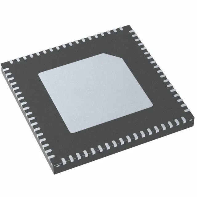
The 72-VFQFN Exposed Pad (10x10 mm body,) provides a central thermal pad for heat sinking to the PCB ground plane. The exposed paddle must be soldered to a copper pour with sufficient vias to the inner layers — without a low-thermal-resistance path, the junction temperature rises above the 85°C ambient limit, especially when all twenty outputs are switching at 250 MHz. The tape-and-reel packaging supports automated pick-and-place; cut-tape samples are also available for prototyping.
No pin-compatible second source is recorded — the fanout ratio and HCSL output type are specific to this Microchip device.