Microchip Technology ZL40250LDG1 — Discrete Semiconductors

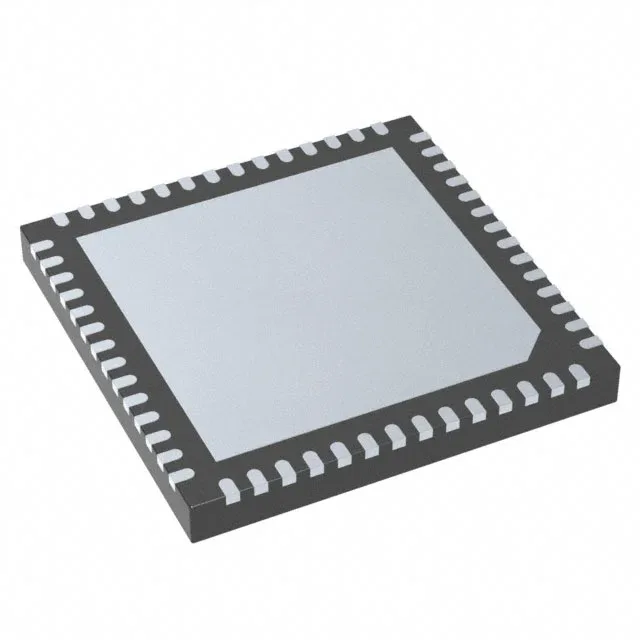
Microchip ZL40250LDG1 SmartBuffer, 1.035 GHz, 56-QFN

MPNZL40250LDG1
End of Life

Microchip Technology SmartBuffer™ Fanout Buffer (Distribution), Divider, Multiplexer, ZL40250LDG1, 1.035 GHz max, 4:6 I/O, differential I/O, 1.71-3.465 V, -40 to 85°C, 56-VFQFN Exposed Pad, Tray.

$8.82Ref. price · indicative, final on quote
Packaging56-VFQFN Exposed Pad
RoHSROHS3 Compliant
SeriesSmartBuffer™
Independent supplier — new & surplus stockAuthenticity-screened · ESD-safe packingListing updated Aug 2026

Specifications

ZL40250LDG1 specifications
ParameterValue
TypeFanout Buffer (Distribution), Divider, Multiplexer
SeriesSmartBuffer™
MountingSurface Mount
Supply voltage1.71V ~ 3.465V
Frequency - max1.035 GHz
Operating temperature-40°C ~ 85°C
InputCMOS, Crystal
OutputCML, CMOS, HCSL, HSTL, LVDS, LVPECL, SSTL
PackageTray
Case56-VFQFN Exposed Pad
Number of circuits1
Ratio - Input:Output4:6
Differential - Input:OutputYes/Yes

Product details

Clock-tree glue that handles any output standard

The ZL40250LDG1 is a programmable fanout buffer from Microchip's SmartBuffer™ family, combining distribution, divider, and multiplexer functions in a single 56-QFN package. It accepts CMOS or crystal inputs and delivers up to six copies of the clock across any of eight output standards — CML, CMOS, HCSL, HSTL, LVDS, LVPECL, or SSTL — without needing external level translators. The 4:6 input-to-output ratio means four independent input paths feed six outputs, with full differential support on both sides. At 1.035 GHz maximum frequency, this part covers the upper end of high-speed serial clocks (PCIe Gen4/5 reference, 10GbE, Fibre Channel) without hitting the ceiling.

Supply flexibility and temperature range for mixed-voltage boards

The wide range means a single BOM line can serve designs that transition between core and I/O voltages, reducing the number of unique regulator outputs. The 56-VFQFN with exposed pad (8x8 mm) demands a solid thermal via pattern under the paddle to keep junction temperatures in check at the upper end of the range.

For new designs, this part is a safe selection — no near-term LTB risk.

Frequently asked questions

What output standards does the ZL40250LDG1 support?

It supports CML, CMOS, HCSL, HSTL, LVDS, LVPECL, and SSTL outputs. This lets the same buffer drive a PCIe clock (HCSL), an FPGA reference (LVDS), and a backplane signal (LVPECL) without external conversion.

Is the ZL40250LDG1 RoHS compliant?

Yes, it is ROHS3 compliant per Microchip's listing.