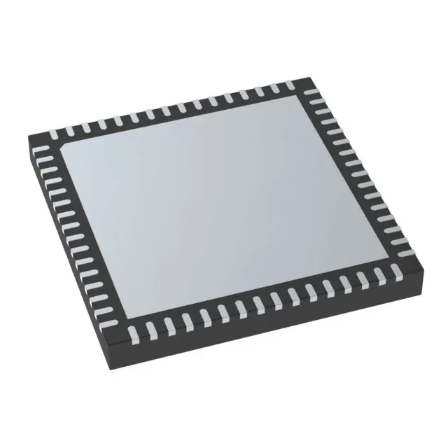
What this PLL brings to a line-card or base-station clock tree
The Microchip ZL30641LDG1S is a single-channel PLL clock generator designed for Ethernet, SONET/SDH, and wireless base station timing. It accepts up to five CMOS or differential inputs and delivers ten outputs in CMOS, LVDS, or LVPECL formats, with a maximum output frequency of 750 MHz. The fully differential signal path (input and output) keeps jitter low enough for 10GbE and CPRI reference clocks. Dual supply rails — 1.8 V and 3.3 V — let it sit on a mixed-voltage board without an extra regulator.
The 750 MHz maximum output frequency covers most Ethernet MAC/PHY reference clocks (125 MHz, 156.25 MHz), SONET/SDH line rates up to OC-192 (622.08 MHz), and wireless base-station local oscillators in the 491.52 MHz to 737.28 MHz range. If your design needs a 1 GHz+ clock for a 100GbE gearbox or a JESD204B converter, you'd step up to a multi-PLL part like the ZL30793LFG7, which runs to 1045 MHz and adds HCSL and HSTL output options.
Output format flexibility saves board space
CMOS, LVDS, and LVPECL on the same device means one BOM line covers the FPGA bank (LVDS), the SerDes reference (LVPECL), and the general-purpose logic fan-out (CMOS). No external level translators or redundant oscillators. The 5:10 input-to-output ratio gives plenty of fan-out for a line card without adding a separate clock buffer.
Package and power — what the layout engineer sees
Supply decoupling should cover both the 1.8 V and 3.3 V rails with 0.1 µF and 1 µF caps per pin group, as recommended in the layout guide. Surface-mount only; no through-hole option.
New designs can commit to it without a near-term obsolescence concern.