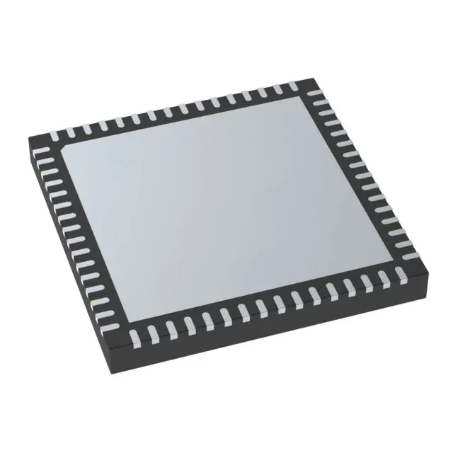
Clock synthesis with integrated PLL for line-card timing
The ZL30631LDG1 is a single-channel SyncE timing IC from Microchip, built around an integrated PLL that generates and cleans up clocks for Ethernet, SONET/SDH, and wireless base station line cards. Its 5:10 input-to-output ratio allows redundant reference selection and fan-out to multiple PHYs or FPGAs from one device, reducing BOM count on a timing blade.
750 MHz differential outputs and dual supply rails
The part accepts a CMOS reference input and delivers up to ten outputs in CMOS, LVDS, or LVPECL formats, with a maximum output frequency of 750 MHz — fast enough to clock 10GbE SERDES or JESD204B converters directly. Both input and output paths support differential signaling, so the device can accept a differential reference and distribute low-jitter differential clocks without external level translation. Dual supply voltages of 1.8 V and 3.3 V let the core run at the lower rail while the output buffers swing at the higher level, matching the I/O voltage of the downstream load.