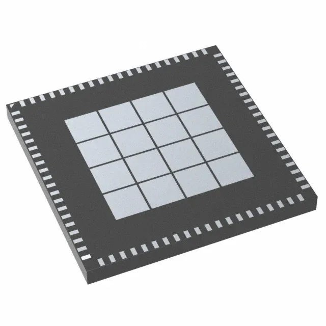
Microchip Technology ZL30256LFG7 — Discrete Semiconductors

Microchip ZL30256LFG7 Jitter Attenuator, 1.045 GHz, 80-LGA

MPNZL30256LFG7
End of Life

Microchip Technology ZL30256LFG7 jitter attenuator, PLL-based, 1.045 GHz max, 10:18 I/O, 3 circuits, CMOS/HCSL/HSTL/LVDS/LVPECL outputs, 80-LGA (11x11 mm), tray.

$31.46Ref. price · indicative, final on quote
Packaging80-VFLGA
Independent supplier — new & surplus stockAuthenticity-screened · ESD-safe packingListing updated Aug 2026

Specifications

ZL30256LFG7 specifications
ParameterValue
TypeJitter Attenuator
MountingSurface Mount
Supply voltage1.71V ~ 1.89V, 3.135V ~ 3.465V
Frequency - max1.045GHz
Operating temperature-40°C ~ 85°C (TA)
PLLYes
InputCMOS
OutputCMOS, HCSL, HSTL, LVDS, LVPECL
PackageTray
Case80-VFLGA
Divider (Multiplier)Yes/No
Number of circuits3
Ratio - Input:Output10:18
Differential - Input:OutputYes/Yes

Product details

PLL-based jitter cleaning for high-speed clocks

The ZL30256LFG7 is a PLL-based jitter attenuator from Microchip, designed to clean up noisy clock sources in high-speed digital systems. It accepts a single-ended CMOS input and can produce up to 18 outputs in any mix of CMOS, HCSL, HSTL, LVDS, or LVPECL standards — covering the common logic families used on a typical FPGA or SerDes reference clock tree. With a maximum output frequency of 1.045 GHz, this part handles 10G-class SerDes reference clocks and high-speed ADC/DAC sample clocks. The three independent PLL circuits let you clean multiple clock domains from a single device, reducing board space and BOM count compared to using separate attenuators per rail.

80-LGA package and board integration

The 1.71V–1.89V core supply and 3.135V–3.465V I/O supply rails are separate, so you can run the core at 1.8V while the outputs swing at 3.3V to match downstream logic levels. The differential input and output capability means it can accept and deliver LVDS or LVPECL signals directly, avoiding external level translators.

Frequently asked questions

What output standards does the ZL30256LFG7 support?

The device outputs CMOS, HCSL, HSTL, LVDS, and LVPECL. This covers the common clock formats for FPGAs, SerDes, and high-speed converters, so you can drive multiple logic families from one attenuator.

What is the maximum frequency the ZL30256LFG7 can generate?

The maximum output frequency is 1.045 GHz, which covers 10G-class SerDes reference clocks and high-speed ADC/DAC sample rates.