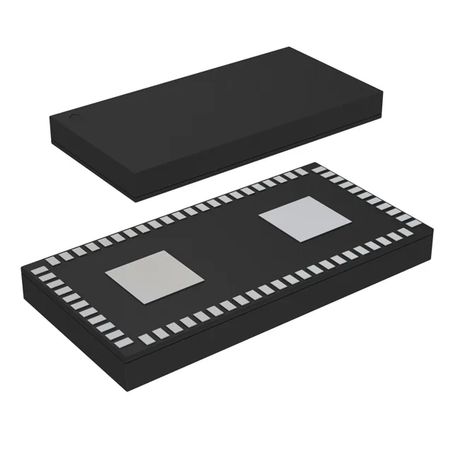
Dual PLL engine for multi-rate clock trees
The ZL30245LFG7 is a clock multiplier and frequency synthesizer from Microchip Technology, built around two independent PLL circuits with a bypass mode. It accepts CMOS or crystal inputs and produces CML or CMOS outputs, making it a flexible clock source for systems that need to generate multiple clean frequency domains from a single reference. With a maximum output frequency of 1.035 GHz, this part is sized for high-speed serial interfaces like 10GbE, Fibre Channel, or PCIe reference clocks where jitter and phase noise matter. The 4:3 input-to-output ratio means you can feed three independent clock lanes from four reference sources, or use the spare input for a redundant failover reference.
Supply flexibility and temperature grade
This wide tolerance simplifies power rail design in mixed-voltage systems where the clock IC sits between an FPGA core and I/O bank.
No additional compliance documentation (REACH, UL, IEC) is listed in the available records; standard Microchip material declarations are available on request.