What the PLL and 100 MHz ceiling mean for your clock tree
The ZL30110LDF1 is a telecom-grade digital PLL (DPLL) with a 100 MHz maximum output frequency, purpose-built for rate conversion in synchronous networks. The integrated PLL cleans jitter from the reference clock and synthesises a low-phase-noise output at the target frequency, up to 100 MHz. For a line card or base station clock tree, this means one device replaces a discrete VCXO + PLL loop — the DPLL handles both frequency synthesis and wander filtering in the digital domain. The 2:4 input-to-output ratio gives you two reference inputs (LVCMOS or crystal,) that can be switched or held as a primary/backup pair, feeding four LVCMOS clock outputs. Non-differential I/O keeps the routing single-ended — simpler board layout than CML or LVPECL, but the trace impedance and length matching still matter at 100 MHz to avoid reflections.
Package, supply, and temperature — board-fit checklist
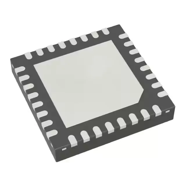
The supply rail is 3.1V to 3.5V — a clean 3.3V rail with <50 mV ripple is the typical choice; the DPLL's internal regulator rejects some supply noise, but the VCO's phase noise floor tracks the rail quality. Single-circuit device — one PLL core per package. Surface-mount assembly with MSL level typical for QFN packages; the exposed pad must be soldered to the ground plane for both thermal and electrical reference. The 32-QFN footprint is shared across the ZL3011x family, so a board layout for the sibling parts accepts this device without change.
Active lifecycle and compliance — procurement posture
ROHS3 compliant, which covers the current EU exemption scope for lead-free assembly. The active status means the factory continues to produce the device, so multi-year design support is expected without a forced migration.