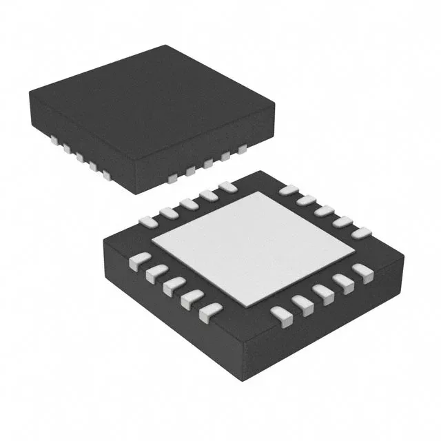
The UCS2112-1-V/G4 comes in a 20-VFQFN with an exposed pad, 4x4 mm footprint. If the pad is not soldered to a copper plane with thermal vias, the junction temperature climbs past the 105°C ambient rating and the part enters thermal shutdown at a lower output current than the 3 A spec suggests. The package ships in Tube format, not tape-and-reel. For high-volume pick-and-place lines that expect embossed tape, this means a tube feeder or a manual changeover — factor that into the assembly planning if the rest of the BOM is reel-fed.
Digital control saves a resistor — but needs firmware before the port turns on
The switch is controlled over I²C or SMBus, with the host setting the current limit per output through the digital interface rather than an external resistor. That saves a BOM component per channel, but it also means the port stays off until the microcontroller initialises the I²C peripheral and writes the limit register. On a cold boot where the USB port must be live before the firmware runs (e.g., a factory-default charging port), the default power-on state of the outputs needs to be checked against the system requirement. The adjustable current limit and UVLO are both configured over the bus. If the I²C lines are shared with other devices, a bus stall or address collision leaves the switch in its last state — the outputs do not default to a safe-off condition unless the firmware explicitly sets them that way.
Two 3 A outputs — sizing for USB and beyond
Each of the two high-side outputs delivers up to 3 A continuously, with a 1:1 input-to-output ratio — each output is an independent switch, not a mux. At 3 A per channel, the 40 mOhm Rds(on) produces a 120 mV drop — inside the 250 mV drop budget that USB 2.0 allows from the host port to the connector. For USB 3.0 at 900 mA, the drop is only 36 mV, leaving headroom for cable and connector losses.