Load-switching polarity and voltage ceiling
The TP2104N3-G-P003: The P-Channel polarity means the load connects between the drain and ground, with the source tied to the positive rail — the gate is pulled low to turn the FET on, making it a natural fit for high-side load switching in battery-powered or positive-rail systems where an N-Channel would require a charge-pump driver.
On-resistance and conduction loss budget
Maximum Rds(on) is 6 Ohms at 500 mA drain current with a 10 V gate drive. At the rated 175 mA continuous current, the conduction loss is I²R = 0.175² × 6 ≈ 184 mW — about a quarter of the 740 mW power dissipation budget at 25°C ambient.
Thermal envelope and junction temperature margin
The 740 mW power dissipation is specified at 25°C ambient in free air; derating applies above that temperature. With the 60 pF input capacitance at 25 V drain-source, the switching losses in a low-frequency load-switch application are negligible compared to the conduction loss — the thermal budget is dominated by the DC current and Rds(on).
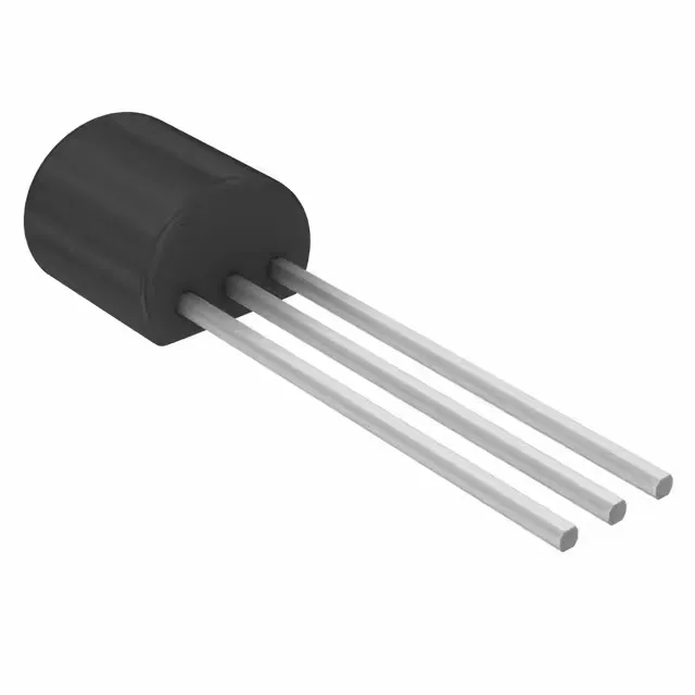
Housed in the TO-92-3 (TO-226AA) through-hole package, the TP2104N3-G-P003 mates with standard 0.100-inch pitch breadboard, perfboard, or PCB layouts. The three leads — gate, drain, source — are arranged in a single in-line row; the supplier device package is TO-92-3. For a 175 mA load, the PCB trace width to the drain and source pads should be sized for at least 0.5 mm to keep the temperature rise below 10°C in still air.
The base product number TP2104 covers the family; the N3 suffix indicates the TO-92 package, G the ROHS-compliant finish, and P003 the packaging option.