What the 1.5A peak output and 25ns rise time mean for your switching stage
The TC4432EOA713 delivers 1.5A peak source and 1.5A peak sink current, with a typical 25ns rise and 33ns fall time driving a 1nF load. That combination means it can charge the gate capacitance of a medium-power MOSFET (say 2-5 nC total gate charge) in under 50 ns — fast enough to keep switching losses in check for a 100-200 kHz SMPS or a motor-drive PWM stage running at 20 kHz. It won't drive a GaN FET or a massive IGBT module, but for the vast majority of TO-220 and D2PAK silicon MOSFETs, this is a solid match. That saves a translator chip and one more trace on the board.
Active lifecycle and what it means for a BOM line
For a procurement team reviewing a BOM for a new design, that means no immediate last-time-buy risk and no forced migration to a successor. The ROHS3 compliance is confirmed, which covers the EU RoHS directive without exemptions. That qualifies it for under-hood or engine-bay electronics, not just cabin or infotainment.
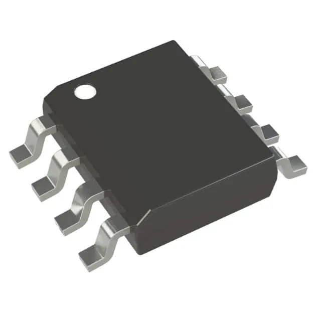
Package and board-fit: 8-SOIC with no thermal pad
There is no exposed thermal pad — the die dissipates through the leadframe and the copper traces. For the 1.5A peak current at a few hundred kHz, the average power dissipation is low enough that a standard SOIC footprint with 1 oz copper pours on the drain pins handles the heat without a dedicated thermal land.