Active production — BOM-fit for low-side gate drive
The TC1428COA: It is a low-side gate driver capable of driving both N-channel and P-channel MOSFETs, with a peak output current of 1.2 A for both source and sink.
Switching speed and drive strength
Typical rise and fall times of 35 ns and 25 ns respectively, into the rated load, set the practical switching ceiling — at 500 kHz the output edges consume roughly 3% of the period, leaving margin for the dead-time window in a synchronous rectifier or push-pull stage. The 1.2 A peak drive current charges the MOSFET gate capacitance quickly; for a typical 10 nC gate charge, the driver transitions the gate in under 10 ns, though the external gate resistor and PCB trace inductance will dominate the actual edge rate.
Package and temperature grade — board-level constraints
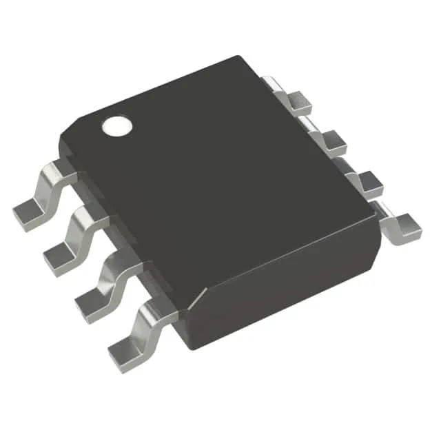
Housed in an 8-lead SOIC package with 1.27 mm pitch, the TC1428COA routes easily on a two-layer board — the supply and output pins are on opposite sides, so the power loop can be kept tight with a local bypass capacitor placed within 5 mm of the VDD and GND pins. Shipping in tube format, the devices are oriented for pick-and-place with the pin-1 indicator at the tube's orientation notch.
Input logic flexibility — inverting and non-inverting
Both inverting and non-inverting inputs are available on independent channels, so a single TC1428COA can drive one MOSFET with the same polarity as the PWM signal and a second with inverted polarity — useful for a synchronous buck where the high-side and low-side gates require complementary signals. The two channels are independent, meaning they can be driven from separate control signals with no cross-coupling — each channel's input is isolated from the other's switching activity.