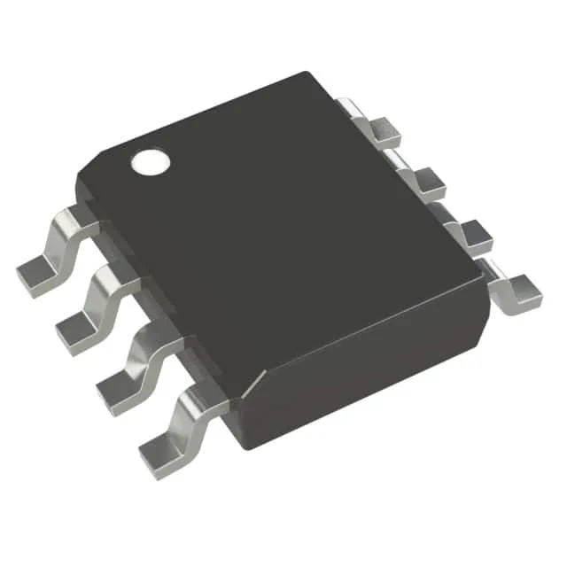
What the 2A peak output buys you on the bench
The TC1412COA713 delivers 2 A peak source and 2 A peak sink current, which means it charges and discharges a typical 1 nF MOSFET gate capacitance in about 18 ns. That rise/fall time keeps switching losses low in a 200-500 kHz DC-DC converter or a motor pre-drive stage — the gate driver's output impedance, not the MOSFET's internal gate resistance, sets the edge rate. It drives both N-channel and P-channel MOSFETs, so you can use it as a low-side pull-down for an N-channel or as a level-shifted high-side driver for a P-channel with a bootstrap diode. The inverting input means a logic high on the input turns the output low — watch the polarity if your controller's PWM output is active-high.
Supply rail and logic compatibility
The logic thresholds are 0.8 V max for VIL and 2.0 V min for VIH, so a 3.3 V microcontroller output drives it directly; no level translator needed between the controller and the driver. Single-channel low-side configuration keeps the layout simple: one bypass capacitor between VDD and GND placed within 5 mm of the pins, and the output trace to the MOSFET gate kept under 20 mm to minimise ringing. The 8-SOIC package is a standard footprint that routes easily on a two-layer board.