Active dual-rail PMIC for space-constrained designs
The TC1303B-DG0EMF: The integrated power sequencer (w/Sequencer = Yes) ensures the two rails come up in the correct order on power-on, eliminating the need for an external supervisor or reset IC in multi-voltage designs.
What the 2 MHz switching and dual topology mean for your BOM
The 2 MHz switching frequency of the synchronous buck converter lets you use small-value inductors and ceramic output capacitors — typically 1 µH to 4.7 µH and 10 µF MLCCs — keeping the total solution footprint under 30 mm² including passives. The LDO output provides a clean, low-noise rail at 2.7 V / 300 mA for analog or RF sections that cannot tolerate the ripple from a switching regulator — the buck's output feeds the LDO's input internally, so the LDO's PSRR attenuates the switching noise. Operating temperature covers -40°C to 85°C, which is the industrial-grade band — suitable for outdoor telecom, factory-floor sensors, and automotive cabin electronics that see ambient heat but not under-hood extremes.
Package, footprint, and board integration
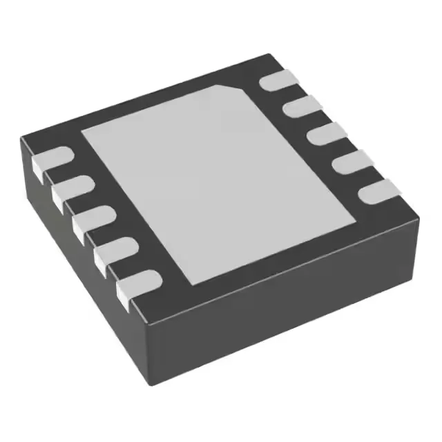
Housed in a 10-VFDFN with exposed pad (3x3 mm DFN per the supplier device package), the part is surface-mount with a thermal pad underneath that must be soldered to a PCB copper land for adequate heat dissipation — the junction-to-board thermal path goes through this pad. The exposed pad also serves as the ground connection; the datasheet layout recommendation places several thermal vias under the pad to pull heat into the inner-layer ground plane. Supplied in tube packaging, which is the standard antistatic tube for DFN devices — suitable for low-volume assembly or prototyping; for reel packaging check the TC1303B-DG0EMFTR variant.