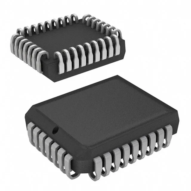
32-PLCC footprint and board-fit
The SST49LF080A-33-4C-NHE-T comes in a 32-lead PLCC (J-lead) package, supplier device package 32-PLCC measuring 11.43x13.97 mm. The J-lead gull-wing footprint suits a standard PLCC-32 socket or direct solder to a PCB pad pattern matching the JEDEC MO-047 outline. Surface-mount assembly with a reflow profile typical for J-lead packages — the lead pitch is wide enough that a two-layer board handles the routing without via stitching under the body.
Parallel interface timing and throughput
This is an 8 Mbit parallel NOR flash organized as 1M x 8 bits. The 120 ns access time sets the ceiling for random read latency — at 33 MHz clock the synchronous burst read can sustain higher throughput, but the first-word access is bound by that 120 ns figure. The write cycle time per word or page is 20 µs, which defines the programming throughput for firmware updates or data logging. Supply voltage range is 3V to 3.6V, so a 3.3V rail with ±5% tolerance keeps the part within spec.