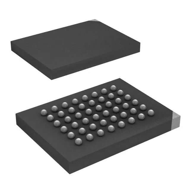
48-ball TFBGA — what the board sees
The SST39VF400A-70-4I-B3KE ships in a 48-TFBGA (Thin Fine-Pitch Ball Grid Array) — 0.75 mm ball pitch, 0.5 mm ball diameter, 8×6 ball matrix. The package height is 1.0 mm max, seated height 0.90 mm typical. The landing pattern calls for 0.35 mm NSMD pads with a 0.45 mm solder-mask opening; the via-in-pad is not required but a 0.2 mm microvia under the ball improves thermal transfer on inner layers. Decoupling: place a single 100 nF X7R 0402 within 2 mm of each VDD ball pair (balls A1, A8, B4, B5, D4, D5, F4, F5, G1, G8).
70 ns access — what it buys the firmware team
70 ns access time means the device outputs valid data 70 ns after the address lines settle and CE# goes low. For a 50 MHz bus master with a 20 ns clock period, the flash must be ready within 3.5 clock edges — a 70 ns access fits comfortably into a single 100 MHz cycle with margin for PCB trace delay. The 256K × 16 organization maps directly to a 512 KB address space — the upper address line (A18) selects the upper or lower 256K word. The parallel interface uses a 19-bit address bus and 16-bit data bus; no address multiplexing is needed, so the firmware sees a flat memory map with no page register overhead. Word write cycle time is 20 µs typical — a full 256K-word firmware image takes roughly 5 seconds to program at the word-write rate.
Industrial temperature and supply — fit for the enclosure
A PLC I/O module or motor drive controller that sees 70°C internal air temperature still has 15°C margin before the flash hits its upper limit. The SST39 MPF™ series uses Microchip's SuperFlash technology — sector erase time is 18 ms typical, full-chip erase 70 ms typical. The 4 Mbit density is a common code-storage size for bootloaders and configuration tables in industrial controllers where a serial flash would add latency on every read.
No official second-source or pin-compatible cross-reference is listed. The parallel NOR flash market has few drop-in alternatives at this density and package — the AT24C08D-SSHM-B (8 Kbit serial EEPROM, I²C) and 24AA128T-I/SN (128 Kbit serial EEPROM, I²C) are different interface types and densities, not functional replacements. The 23K640-I/SN (64 Kbit SPI SRAM) is volatile — not a flash substitute.