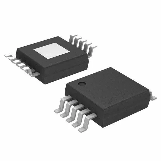
2 A, 2 MHz buck in a 10-MSOP-EP footprint
The MIC4720YMME: The output is adjustable from 1 V up to the input voltage.
Switching frequency and inductor selection
At 2 MHz, the switching period is 500 ns. The internal high-side switch has a typical minimum on-time around 100 ns, which limits the minimum duty cycle to about 20 % at 2 MHz. For a 5 V input generating a 1 V output (20 % duty), the part runs at the edge of the minimum on-time — a lower switching frequency or higher output voltage avoids pulse-skipping. The 2 MHz rate pushes the fundamental switching noise above the AM radio band, which simplifies filtering in noise-sensitive designs.
Thermal design with the exposed pad
The 10-MSOP-EP package relies on the exposed pad (EP) as the primary heat path. At 2 A output from 5 V to 3.3 V (about 3.4 W input, 6.6 W output, ~1.4 W loss in the regulator), the junction-to-ambient thermal resistance with a proper PCB pad and via array is typically 40–50 °C/W. Without the EP soldered to a copper plane, the junction temperature exceeds the 125 °C limit at room ambient. The layout must connect the EP to the ground plane with at least four thermal vias, and the copper area under the part should be at least 300 mm² on the top layer.
No official pin-compatible second source or successor is listed, so the BOM should be qualified with this single source.