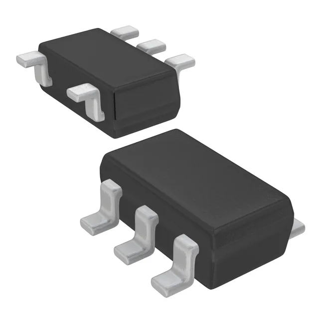
Microchip Technology MCP6V86UT-E/LTY — Memory (DRAM / SRAM / Flash / EEPROM)

MCP6V86UT-E/LTY Zero-Drift Op-Amp, 5 MHz GBWP, SC-70-5

MPNMCP6V86UT-E/LTY
End of Life

Microchip Zero-Drift series, MCP6V86UT-E/LTY, chopper (zero-drift) op-amp, 1 circuit, 5 MHz gain bandwidth, 4 V/µs slew rate, rail-to-rail output, 2.5 V to 5.5 V supply, SC-70-5 package, -40°C to 125°C.

$1.29Ref. price · indicative, final on quote
Packaging5-TSSOP, SC-70-5, SOT-353
StockContact for availability
MOQ1 pcs
  • 100% new & originalTraceable channels only — no refurbs, no pulls, no remarked parts.
  • Date & lot codes on quoteStated per line before you commit; label photos on request.
  • MSL-compliant ESD packingMoisture-sealed bags with indicator cards; reels photo-verified.
  • PayPal buyer protectionPay by T/T, PayPal or Payoneer — card payments covered end to end.

Specifications

MCP6V86UT-E/LTY Technical Specifications
ParameterValue
SeriesZero-Drift
Output typeRail-to-Rail
Mounting typeSurface Mount
Amplifier typeChopper (Zero-Drift)
Voltage - input offset25 µV
Voltage - supply span5.5 V
Current - supply500µA
Current - input bias2 pA
Current - output (Channel)40 mA
Operating temperature-40°C ~ 125°C
Gain bandwidth product5 MHz
PackageTape & Reel (TR); Cut Tape (CT)
Slew rate4V/µs
Case5-TSSOP, SC-70-5, SOT-353
Number of circuits1

Product details

Precision zero-drift op-amp for industrial sensing

The Microchip MCP6V86UT-E/LTY is a single-channel zero-drift (chopper) operational amplifier from the Zero-Drift series, designed to deliver low offset and drift over temperature without the need for external trimming. It combines a 5 MHz gain-bandwidth product with a 4 V/µs slew rate, making it suitable for precision signal conditioning in sensor front-ends, current-sense amplifiers, and data-acquisition paths where DC accuracy matters. The rail-to-rail output stage maximizes dynamic range on low-voltage supplies, and the 2 pA typical input bias current preserves signal integrity when interfacing with high-impedance sources like photodiodes or pH probes.

Key specs for the BOM decision

The 25 µV maximum input offset voltage is the headline figure that defines this part's precision class — it eliminates the need for offset-nulling potentiometers or software calibration in most DC-coupled applications. The 2 pA bias current means the voltage error from a 10 kΩ source is just 20 nV, negligible even in microvolt-level measurements. Output drive capability of 40 mA per channel is enough to swing a 2 V signal into a 50 Ω load or drive the reference input of a successive-approximation ADC directly.

Package and footprint reality

Housed in a 5-lead SC-70-5 (SOT-353) package, this part fits into tight PCB layouts where board area is at a premium. The surface-mount footprint is standard for the SC-70 family, and the small body means careful stencil design for solder-paste volume — a 0.1 mm thickness is typical. No exposed thermal pad, so thermal dissipation relies on the leadframe and copper pours on the PCB.

Lifecycle and compliance

ROHS3 compliant per the compliance record, which covers the current RoHS exemption list without requiring a separate lead-free qualification step.

Frequently asked questions

Is MCP6V86UT-E/LTY RoHS compliant?

Yes, it is listed as ROHS3 Compliant, covering the current RoHS exemption categories.