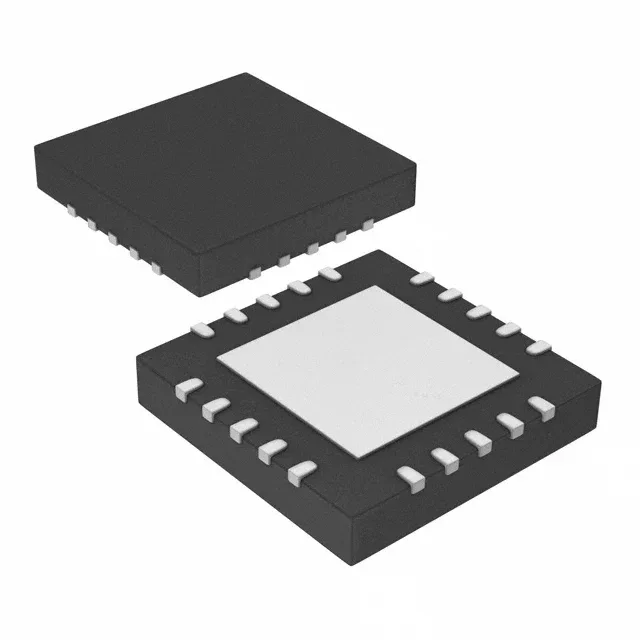
The MCP48FEB14-E/MQ is a quad-channel, 10-bit digital-to-analog converter from Microchip's Automotive AEC-Q100 series, packing four independent DACs with on-chip EEPROM into a 20-VQFN (5x5 mm) package. It's built for applications that need to hold calibration or setpoint values across power cycles without external nonvolatile memory. The 10-bit resolution delivers 1024 discrete output levels; with a 5 V reference that's about 4.88 mV per step. The quad-channel count means one part handles four analog trim or control loops — a BOM consolidation move vs using four single DACs.
Accuracy and speed — INL, DNL, settling time
Integral nonlinearity is ±0.4 LSB typical — that's less than half an LSB of worst-case bow across the full output range. For a 0-5 V span, the output stays within about 2 mV of the ideal transfer function. Differential nonlinearity is ±0.05 LSB typical, guaranteeing monotonicity: every increase in digital code produces a positive voltage step, no missing codes. That matters in closed-loop servo or valve control where a non-monotonic DAC can cause oscillation. Settling time to ±0.5 LSB is 7.8 µs typical. That sets the maximum update rate at roughly 128 kHz for a full-scale step. In practice, small code changes settle faster — the 7.8 µs figure is the worst-case transition. For a 1 kHz control loop, that's nearly 128x margin. The SPI data interface runs at standard clock rates; the 10-bit word length means each channel update takes 16 clock cycles (including the command byte). At 10 MHz SPI clock, that's 1.6 µs per channel — the settling time, not the SPI transfer, is the bottleneck.
Supply rails, temperature range, and automotive qualification
No separate AVDD/DVDD sequencing required. The external reference input accepts voltages up to VDD, giving a rail-to-rail output span when the reference equals the supply. Operating temperature spans -40°C to +125°C, covering the full automotive Grade 1 range. The AEC-Q100 qualification means it's passed the reliability stress tests (high-temperature operating life, temperature cycling, ESD) required for under-hood and engine-bay electronics. The output is voltage-unbuffered — the DAC's output impedance is the R-2R ladder resistance (typical 10 kΩ). That means the load impedance must be >> 10 kΩ to avoid gain error. If driving a low-impedance input, buffer it with an op-amp.
Package, footprint, and thermal management
The 20-VQFN package with exposed pad (5x5 mm body) requires a thermal land on the PCB — the datasheet recommends a 4x4 mm pad with via array to the ground plane. Surface-mount only — no through-hole variant. The 0.5 mm pitch QFN demands a solder stencil with 0.25 mm apertures and a reflow profile peaking at 260°C.
Sourcing and lifecycle — active, no EOL risk
Sourced through authorized distribution channels. No minimum order quantity restrictions beyond standard distributor terms.