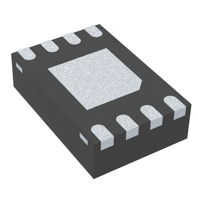
Microchip Technology MCP1725T-ADJE/MC — Power Management (PMIC / Gate Driver)

MCP1725T-ADJE/MC LDO, 500mA, Adjustable, 60dB PSRR

MPNMCP1725T-ADJE/MC
End of Life

Microchip Technology MCP1725T-ADJE/MC adjustable LDO, 500mA, 60dB PSRR at 100Hz, 0.35V dropout, 8-VFDFN exposed pad, -40°C to 125°C.

$0.71Ref. price · indicative, final on quote
Packaging8-VFDFN Exposed Pad
RoHSROHS3 Compliant
Independent supplier — new & surplus stockAuthenticity-screened · ESD-safe packingListing updated Aug 2026

Specifications

MCP1725T-ADJE/MC specifications
ParameterValue
Output typeAdjustable
MountingSurface Mount
Voltage - input6V
Voltage dropout0.35V @ 500mA
Voltage - output5V
Voltage - output (Min (Fixed))0.8V
Output current500mA
Current - quiescent220 µA
Operating temperature-40°C ~ 125°C
PSRR60dB (100Hz)
PackageTape & Reel (TR); Cut Tape (CT)
Case8-VFDFN Exposed Pad
Control featuresEnable, Power Good
Protection featuresOver Temperature, Short Circuit, Under Voltage Lockout (UVLO)
Number of regulators1
Output configurationPositive

Product details

60 dB PSRR at 100 Hz — what it means for the supply rail

The MCP1725T-ADJE/MC delivers 60 dB of power-supply rejection at 100 Hz, which attenuates 100 mV of input ripple to roughly 100 µV at the output. For an ADC reference or analog front-end sharing a rail with a switching converter, this keeps the noise floor from coupling into the signal chain.

500 mA with 0.35 V dropout — headroom budget

At the full 500 mA load, the maximum dropout is 0.35 V — the input rail must stay at least 0.35 V above the set output voltage across temperature and load to maintain regulation. For a 3.3 V output, the input needs at least 3.65 V; a 5 V rail with 10 % tolerance (4.5 V min) still leaves margin. Quiescent current is 220 µA typical, which is low enough for always-on domains in battery equipment but not ultra-low-power — a design targeting single-digit microamp standby should look at the MCP1700 or MCP1811 families instead.

Industrial temp range and protection set

The 8-VFDFN exposed-pad package (2x3 mm DFN) requires a thermal via array under the pad to keep RθJA below 60°C/W in still air. Built-in over-temperature shutdown, short-circuit protection, and under-voltage lockout (UVLO) eliminate the need for external supervisory ICs in most designs. The Enable and Power Good control pins allow sequenced power-up and rail monitoring without extra logic.

Frequently asked questions

What does 60 dB PSRR at 100 Hz mean for my circuit?

60 dB rejection at 100 Hz means the LDO attenuates 100 mV of input ripple to about 100 µV at the output. This is the dominant frequency for full-wave-rectified mains hum (100/120 Hz) and is where many LDOs have their best rejection. The MCP1725T-ADJE/MC's 60 dB at 100 Hz is typical for a general-purpose LDO; expect rejection to roll off above 10 kHz, so a ceramic input cap with low ESL is still needed to shunt high-frequency switching noise.

What is the closest pin-compatible alternative to MCP1725T-ADJE/MC?

The MCP1725 family shares the same die but different package variants; verify the pinout and enable polarity before substituting another order code.