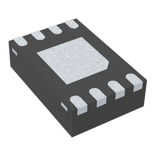
Package and board-fit note
The MCP1725T-1202E/MC comes in an 8-VFDFN exposed-pad package (supplier device package 8-DFN 2x3 mm). The exposed pad on the underside must be soldered to a thermal land on the PCB — the datasheet's recommended footprint ties this pad to the ground plane to pull heat out of the die. Without that thermal via array, the 500 mA output at high ambient will push the junction above the 125 °C rated limit. The tape-and-reel packaging suits automated pick-and-place; the cut-tape option is available for prototype or low-volume builds.
Dropout margin and PSRR — what they mean for the rail
Maximum dropout voltage is 0.35 V at the full 500 mA load. PSRR is 60 dB at 100 Hz — typical for a linear regulator in this class. At 100 Hz the regulator attenuates input ripple by a factor of 1000, which cleans up the residual 100/120 Hz hum from a rectified mains supply. Above a few hundred kHz the PSRR rolls off, so the regulator alone cannot suppress high-frequency switching noise from a preceding DC-DC converter without additional filtering.
Protection and control features
Built-in over-temperature shutdown, short-circuit current limiting, and under-voltage lockout (UVLO) protect the load and the regulator. The UVLO threshold prevents the output from sourcing current when the input rail is too low to maintain regulation — avoids the pass transistor operating in dropout at high current, which stresses the die. The Enable and Power Good control pins allow sequencing: the Enable pin shuts the output off (drawing 220 µA quiescent), and the Power Good flag can drive a reset or enable a downstream converter once the output is within tolerance.