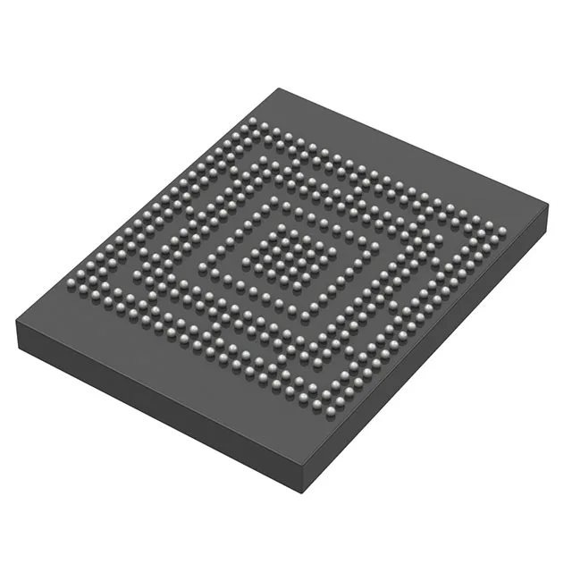
Microchip Technology M2S090TS-1FCS325I — FPGA / CPLD & Programmable Logic

Microchip M2S090TS-1FCS325I SmartFusion2 SoC FPGA, 90K LEs

MPNM2S090TS-1FCS325I
Active

Microchip SmartFusion®2 M2S090TS-1FCS325I, SoC FPGA with ARM Cortex-M3 MCU at 166 MHz, 90K logic modules, 512KB eSRAM, 180 I/O, -40°C to 100°C (TJ), 325-ball BGA.

$242.28Ref. price · indicative, final on quote
Independent supplier — new & surplus stockAuthenticity-screened · ESD-safe packingListing updated Aug 2026

Specifications

M2S090TS-1FCS325I specifications
ParameterValue
SeriesSmartFusion®2
Frequency166 MHz
Operating temperature high-40°C to 100°C (TJ)
Cpu_coreARM® Cortex®-M3
Frame_size512KB
Fuse_speed166 MHz
ArchitectureMCU, FPGA
ConnectivityCANbus, Ethernet, I²C, SPI, UART/USART, USB
Package_typeTray
Number of i (O)180
StatusActive
Peripheral_typesDDR, PCIe, SERDES
Primary attributesFPGA - 90K Logic Modules

Product details

SoC FPGA with a Cortex-M3 and 90K logic modules

The Microchip M2S090TS-1FCS325I is a SmartFusion®2 SoC FPGA that integrates an ARM® Cortex®-M3 processor with FPGA fabric rated at 90K logic modules. The Cortex-M3 runs at 166 MHz and the device carries 512KB of embedded SRAM for code and data. This is the part a system architect reaches for when a single-chip solution needs both deterministic hardware acceleration and a general-purpose MCU core — think industrial motor control with custom PWM generation, or a multi-protocol gateway that handles CANbus, Ethernet, and USB on one die.

180 I/O in a 325-ball BGA — board-level fit

The 325-ball BGA (FCS325 package) brings out 180 user I/O. That is enough for a parallel address/data bus to external DDR memory plus a handful of SERDES lanes and general-purpose FPGA I/O. The 0.80 mm ball pitch is manageable on a 4-layer board with blind vias; a 6-layer stack-up gives cleaner fan-out for the high-speed SERDES pairs.

Connectivity and peripheral headroom

The FPGA fabric adds DDR controllers, PCIe, and SERDES — so the part can talk to a backplane or a high-speed camera sensor without external bridge chips. The 512KB eSRAM is shared between the MCU and the FPGA fabric, which avoids the latency of off-chip memory for small buffers but means the firmware team needs to partition the memory map early in the design cycle.

Frequently asked questions

What is the difference between M2S090TS and M2S090T?

The 'TS' suffix in M2S090TS-1FCS325I indicates a specific temperature grade and package variant within the SmartFusion2 family. The M2S090T (without 'S') typically refers to a different speed grade or temperature range — the exact difference is detailed in the Microchip ordering guide.

When sourcing M2S090TS-1FCS325I, what is the closest functional second-source?

The M2S005-FGG484I is a smaller-density sibling in the same SmartFusion2 family — it uses the same Cortex-M3 core at 166 MHz but has only 5K logic modules and 128KB eSRAM, with 209 I/O in a 484-ball BGA. It is not a pin-compatible drop-in, but the architecture and peripheral set are identical, so firmware and FPGA code can migrate with a board respin.

How do I get current pricing and availability for M2S090TS-1FCS325I?

Submit an RFQ with your target quantity and delivery window — availability and current market pricing will be returned against that request.