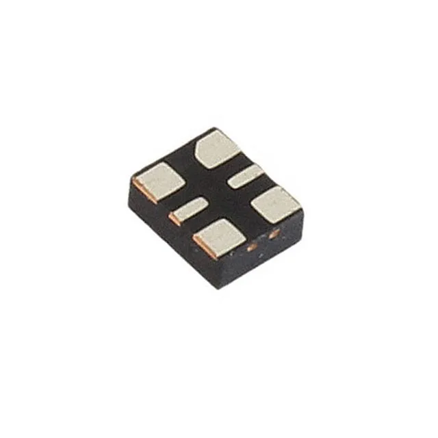
What the LVDS output and MEMS resonator mean for your clock tree
The DSC8123CI2-PROGRAMMABLE: LVDS gives you a low-jitter, low-swing differential signal that drives longer board traces and multiple loads without the common-mode noise pickup you get with single-ended clocks. If you are clocking a high-speed ADC, FPGA, or SerDes transceiver, the LVDS pair keeps the signal clean across the board. Max supply current is 32 mA — modest for an LVDS oscillator, but worth budgeting in a power-sensitive design.
Temperature grade, automotive qualification, and package fit
The AEC-Q100 rating means it passed the full suite of automotive stress tests: temperature cycling, moisture resistance, mechanical shock, and ESD. For a clock source in an engine control unit or ADAS sensor module, that qualification saves you from having to run your own reliability validation. No exposed paddle, so the thermal path is through the solder pads; keep the ground plane under the part for best thermal and electrical performance.
Lifecycle and sourcing — active, no end-of-life concern
Sourced through authorized distribution channels.