Active production — no last-time-buy deadline
The DSC8123BI2-PROGRAMMABLE: This part is a current-production item, not a phase-out or NRND candidate. That means it remains eligible for new design-ins and production builds without a forced migration timeline. The OEM auditor or supply-chain planner can commit this order code to a multi-year BOM with confidence.
AEC-Q100 Grade 2 — the automotive qualification that matters
This XO carries a Ratings entry of AEC-Q100, the automotive IC qualification standard. That certifies the part has passed stress tests for temperature cycling, ESD, latch-up, and reliability per the AEC-Q100 flow — it is not an 'industrial part dressed up as automotive-capable.'. The qualification documentation (PPAP-level data) is available from Microchip for OEM submissions.
LVDS output and MEMS resonator — signal integrity in harsh environments
The LVDS output delivers a differential clock signal with low swing (350 mV typical) and common-mode noise rejection, making it suitable for driving long traces or backplane clock distribution without the EMI footprint of a single-ended CMOS oscillator. This supports power-down or sleep modes without a separate clock gating IC.
Supply voltage and frequency range — parametric flexibility
The available frequency range is 10 MHz to 460 MHz, covering common serial-link reference clocks (25 MHz, 50 MHz, 100 MHz, 125 MHz, 156.25 MHz) and processor core clocks. This keeps the thermal contribution in a dense PCB layout manageable.
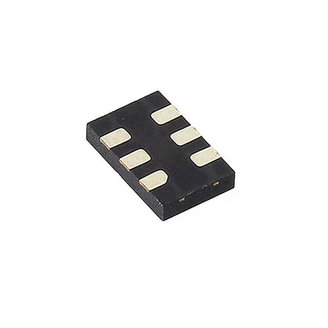
Package and mounting — 6-VDFN with standard footprint
Surface-mount assembly with standard reflow profile. The enable pin is on a standard pinout; the pad layout is symmetrical and non-polarized for the supply pins. No exposed thermal pad — the package relies on the PCB copper pour under the body for heat sinking.