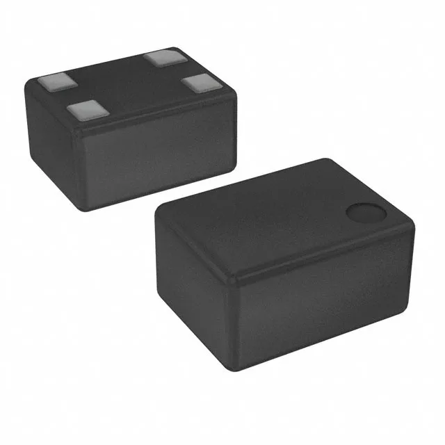
Obsolete dual-output MEMS oscillator — sourcing reality
The DSC6121HI2A-00AMT: This means the manufacturer no longer produces the part; any remaining stock is end-of-life inventory held by distributors or available through surplus channels. For a BOM that requires the 26 MHz and 27 MHz CMOS outputs in a single 4-VFLGA package, the replacement path is a board spin to two single-output oscillators or a different multi-output MEMS clock generator.
What the dual-output and MEMS technology mean for the design
The DSC6121HI2A-00AMT delivers two independent CMOS clock outputs — 26 MHz and 27 MHz — from a single MEMS resonator. This eliminates the need for two separate crystal oscillators on the board, saving PCB area and reducing BOM line count. That is tight enough for most microcontroller clocking, USB interfaces, and Ethernet PHY reference clocks — the jitter budget on a 100BASE-TX PHY typically allows ±50 ppm, so this part provides margin.
This single-sourcing flexibility simplifies inventory — one oscillator part number serves multiple voltage domains on the same board. Maximum current draw is 3 mA typical. At 3.3 V that is under 10 mW total for both clock outputs — negligible in a battery-powered design and well below the thermal budget of the 4-VFLGA package.
The 0.89 mm profile fits under low-clearance shields or in thin handheld enclosures. The CMOS output swings rail-to-rail and drives standard logic inputs directly — no termination resistors or AC-coupling capacitors needed for on-board clock distribution.