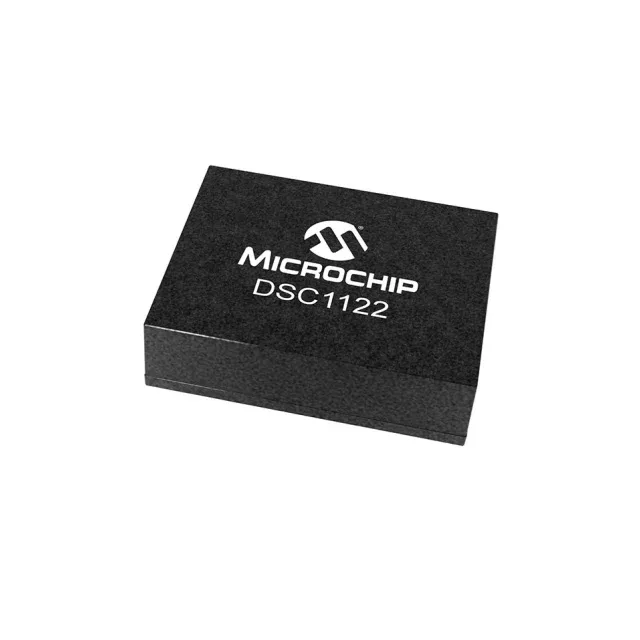
Wide supply range and low power draw
The DSC6101MA3B-032.0000: Typical current consumption is 3 mA max, which keeps the thermal contribution negligible in a dense PCB layout.
The land pattern follows the standard 4-pin LGA footprint; the exposed centre pad should be connected to a ground plane for thermal and mechanical stability. Reflow profile per JEDEC J-STD-020 for moisture-sensitive components applies — bake before rework if the floor life has been exceeded.
Frequency stability and output drive
For a 32 MHz carrier, that translates to a maximum deviation of 640 Hz — well within the tolerance of typical CAN, LIN, or basic Ethernet PHY reference clocks. The CMOS output swings rail-to-rail and drives standard logic loads without external termination.